fmak said:
I find OSCON audio type useful but have not much clear idea why.
Did you compare them soundwise to other types?
In my experience, each cap has certain sonic signature. It doesn't matter where you place it, this signature always comes out.
I Agree with Peter, you can always hear the Sonic effects of Caps – great care has to be taken to reduce their effect in the circuit.
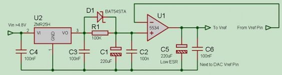
The Vref pin on an ADC/DAC is one of the most critical nodes in a circuit, and is often over looked. Internally, this pin is normally used to supply charge to a Switch capacitor network (in a 1 Bit or Low Bit DAC). The charge is drawn at the internal switching rate – but with an Audio modulation component. Therefore, this Node needs to be well de-coupled at both the Audio Band and “RF” frequencies.
If you where to perform an Impendence plot of any capacitor, you will see a wildly varying curve, with the De-Coupling properties of the capacitor rapidly reducing at LF. This increasing impendence at LF has a large impact on Bass quality – resulting in “1 Bit or Low Bit” DAC’s sounding “light” in the Bass.
Most Vref pins are at half VCC typically 2.5V. The internal Bias generator can only supply a limited current, so there’s no point in hanging large De-coupling caps on them – it will take forever to charge these up – and you will still be left with the Caps varying impendence which will impact its “foot print” on the sound.
The best approach is to add external Very Low Noise and ultra low impedance Vref Generator. Below is a circuit I often use. Pls. note, it’s for designs where Vref is 2.5V. Due to the “High” impedance of the internal Vref (VBias) Gen, they don’t normally mind the addition of the external Gen. Nevertheless; it’s prudent to match the output voltage of the External Generator, as close to the output voltage of the internal Gen as possible.
Due to the Feedback of the OP-AMP, the impedance of the Generator appears almost “flat” within the Audio band (in fact, the output impedance is much LOWER at LF) – thereby limiting the sonic “footprint” of the VRef Capacitor used. Its important to realise that RF decoupling is still required, and the OP-Amp will offer very little correction - due to its limited gain Bandwidth at RF. The RF quality of the 100nF ceramic is critical, try placing it directly across the DAC Vref Pin and Ground – and the electrolytic C5 should be a Low ESR such as an OS-Con or Tant. The quality will now be less critical, due the active correction of the OP-AMP.
Note, the feedback is taken FROM the DAC Vref pin; this removes the effect of PCB wiring and any noise. The limitation at LF is now due to the DAC’s package bonding impendence.
The FB connection should be as short as possible back to the Op-Amp.
Attachments
Did you compare them soundwise to other types?
In my experience, each cap has certain sonic signature. It doesn't matter where you place it, this signature always comes out. [/B][/QUOTE]
------------------------------------------------------------------
This I agree with in analogue systems. I have not the same amount of experience in digital circuits. Where I have used OSCONs (mainly SGs) they have been beneficial. Certainly in clcok circuits, they have a big effect on power supply noise. I have even tried 680 uF/6.3V! No lytic I have tried have the same effect.
Leakage
Leakage currents for filter cap for the reference voltage in combination with 100K filter resistor can cause significant noise at the point where you are trying to filter it. Some of the low ESR caps have fairly high leakage currents Picking a low leakage cap and a smaller resistor is probably worth investigation. One had better be sure that the reference voltage pin of the IC you are driving will work be driven by a low impedance source who's voltage at the reference pin could appear before the ICs power supply votage comes up (depending on supply filtering for the IC and reference circuit. This approach will probably work in many cases but read the ap notes and data sheet thoroughly to avoid possible "got ya"s.
http://www.analog.com/UploadedFiles/Associated_Docs/515815288352085372438388Power_sect2.pdf
Hi Fred,
Thanks for your comments. I don't spec a Low ESR cap for C1 as it would be a waste of money in this postion. Dispite D1's fast "pull-up" action, its almost certain that the external Vref circuit will be slower to reach the correct voltage, then the internal bias Gen - thereby preventing any latch-up conditions - but a good point to be aware of.
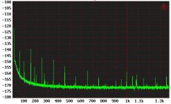
I also checked the noise performance on an FFT, and any noise above 100Hz is below the Zoom FFT noise floor of -170dB ref 2.5V. A good result for such a cheap and simple circuit.")
Thanks for your comments. I don't spec a Low ESR cap for C1 as it would be a waste of money in this postion. Dispite D1's fast "pull-up" action, its almost certain that the external Vref circuit will be slower to reach the correct voltage, then the internal bias Gen - thereby preventing any latch-up conditions - but a good point to be aware of.
I also checked the noise performance on an FFT, and any noise above 100Hz is below the Zoom FFT noise floor of -170dB ref 2.5V. A good result for such a cheap and simple circuit.
I also checked the noise performance on an FFT, and any noise above 100Hz is below the Zoom FFT noise floor of -170dB ref 2.5V. A good result for such a cheap and simple circuit. [/B][/QUOTE]
-------------------------------------------------------------------
Thanks John, I shall try the circuit. Can you pl describe the subjective sonic benefits of it?
I have been looking at power supply interactions with XOs and as an aside did some FFT analysis of XO outputs. They vary enormously and some 'audiophile 'designs have very high odd harmonic contents (-8dB or so third) whilst others have much better suppression (-15dB third and few others). They also vary enormously in wave shapes, some with extremely distorted and asymmetric outputs.
A lot has been made of jitter, never this topic. I wonder how the XO output and waveshape affects the output of the digital streams in the processors.

[/B][/QUOTE]-------------------------------------------------------------------
Thanks John, I shall try the circuit. Can you pl describe the subjective sonic benefits of it?
I have been looking at power supply interactions with XOs and as an aside did some FFT analysis of XO outputs. They vary enormously and some 'audiophile 'designs have very high odd harmonic contents (-8dB or so third) whilst others have much better suppression (-15dB third and few others). They also vary enormously in wave shapes, some with extremely distorted and asymmetric outputs.
A lot has been made of jitter, never this topic. I wonder how the XO output and waveshape affects the output of the digital streams in the processors.
Re: Leakage
http://www.analog.com/UploadedFiles/Associated_Docs/515815288352085372438388Power_sect2.pdf [/B][/QUOTE]
---------------------------------------------------------------------
Very good url; thanks.
John W AD suggests using the AD780 at Vref; claims to improve resolution of ADC by 1 bit. May be worth trying.
FredM
As has been stated, you always hear the sound of a Capacitor, without the external Gen Circuit – they all had their sonic “foot-print”, good in some areas – poor in others.
At the end of the day, I could never find a Cap that “sounded” neutral. With the external VGen circuit, Bass becomes very tight – controlled with no “Bloom” and the sound stage opens up! – best of all cap choice is not such a “No Win” situation.
Its strange how improving the Bass always seems to improve the sound stage???
Below is a Zoom FFT of the output of the circuit 0dB @ 2.5V, note that the Mains harmonics (50Hz / 100Hz etc) are mostly from the R&S UPD05 analyser – its worst in this respect then the AP.
Adding a lower noise Vref is not going to help. The ZMR25H is a noisy 2.5 volt regulator – but its noise is completely filtered by the circuit. The noise towards DC is again due to the UPD05. I don’t believe much could be done to improve the circuits noise performance.
Changing the 5534 to the AD797 might help, but I’ve always had problems getting the 797 stable in unity-gain situations – with mV RF oscillation at about 500MHz (very hard to see on a ordinary Scope). Adding the small value resistor in series with the FB loop didn’t help much - and worsen the noise floor. Add before anybody asks – Yes, the 797 was well de-coupled with ceramic SMD caps across its PSU pins and to ground.
Attachments
Rather than construct a circuit for this, is it possible to use a dedicated highly accurate vref chip for an improvement? Or would this be subject to the same problems?
like this perhaps?
http://www.linear.com/pdf/146010fs.pdf
like this perhaps?
http://www.linear.com/pdf/146010fs.pdf
With the Vref pin - noise is not the only important issue – the foremost reason for using the external VGen circuit is to reduce the VREF impedance across the entire audio band including LF. I’m not aware of any VRef IC that can equal the simple circuit for noise, output impedance – or price.
Rotellian said:Rather than construct a circuit for this, is it possible to use a dedicated highly accurate vref chip for an improvement? Or would this be subject to the same problems?
------------------------------------------------
AD says AD780 does the job.
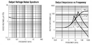
I had a quick look at the LT Voltage reference, and it just goes to supports my earlier Post. The noise is about 1.6uV and output impedance is 2 Ohms @ 100Hz and rises sharply – where its peaks at about 50 Ohms (or worse) @ 10KHz – never a good thing. See the LT Graphs below: -
The output impedance of the Op-Amp VGen circuit will be sub mOhms and have a noise voltage in the nV across the entire audio band – making it hundreds of times better then LT’s integrated voltage reference.
This is not to say that LT’s Voltage reference is bad device – it like most - if not all other Voltage references cannot compete in terms of noise and impedance with the simple Op-Amp VGen. It however will have a very stable output voltage – this is its main function.
In much the same light, the AD780 has a Pk Pk noise of about 20uV 20Hz to 20KHz - and it requires an external Op-Amp buffer to provided low output impendence.
With the Op-amp VGen, you can take the FB from the DAC’S Vref pin as a “Kelvin Sense Node”, thereby guaranteeing the lowest output impedance and noise where its needed.
Also, be aware that there is a dangerous Virus going around. It is called WORK.
If you receive WORK from your colleagues, you’re boss, or anyone else via e-mail or any other means, DO NOT TOUCH IT!
This virus wipes out your private life completely. If you should come into contact with WORK, put on your jacket, take two good friends and go straight to the nearest pub. Order the antidote known as BEER. Take the antidote repeatedly until WORK has been completely eliminated from your system.
Forward this warning immediately to at least 5 friends. Should you realize that you don't have 5 friends, this means that you are already infected and that WORK already controls your life!
Attachments
What's the answer?
Does anyone have a definitive answer on the best capacitor for Vref?
The service manual for my CD624 shows a 6.8uF electrolytic at Vref on the SAA7321 DAC. The Datasheet for the DAC chip shows a 47uF cap.
I am replacing all of the electrolytics in the CDP and am trying to figure out what to use here.
Re: What's the answer?
Use 47 uF OSCON.
--------------------------------------------------------------------Fin said:Does anyone have a definitive answer on the best capacitor for Vref?
The service manual for my CD624 shows a 6.8uF electrolytic at Vref on the SAA7321 DAC. The Datasheet for the DAC chip shows a 47uF cap.
I am replacing all of the electrolytics in the CDP and am trying to figure out what to use here.
Use 47 uF OSCON.
Re: Re: What's the answer?
Should the 100nF bypass cap be removed?
fmak said:
--------------------------------------------------------------------
Use 47 uF OSCON.
Should the 100nF bypass cap be removed?
Hi Fin,
I wouldnt go all the way up to 47uf. The Rotel 965 has a 4.7uf (type F) blackgate here. With a 100nf as well. If you can get hold of it a single blackgate 4.7uf NX HiQ in place of the 100nf (thus nearer the chip - or even better direct from vref pin to gnd pin) might be worth trying. (blackgate usually reported to be better without bypass). Im still looking for a cheap one of these type of players to mess with (a marantz CD42 i acquired doesnt fit the bill so well for tweaking)
I wouldnt go all the way up to 47uf. The Rotel 965 has a 4.7uf (type F) blackgate here. With a 100nf as well. If you can get hold of it a single blackgate 4.7uf NX HiQ in place of the 100nf (thus nearer the chip - or even better direct from vref pin to gnd pin) might be worth trying. (blackgate usually reported to be better without bypass). Im still looking for a cheap one of these type of players to mess with (a marantz CD42 i acquired doesnt fit the bill so well for tweaking)
Re: Re: Re: What's the answer?
Vref should be as stable and low impedance as possible, try 47u with 100n and see if you like it. Ignore what manufacturers do as they try to save money and space.
-------------------------------------Fin said:
Should the 100nF bypass cap be removed?
Vref should be as stable and low impedance as possible, try 47u with 100n and see if you like it. Ignore what manufacturers do as they try to save money and space.
I got it wrong!
Sorry guys, I had another look and the VDDref has a 33uF/16V with a 100nF ceramic - VRC has a 6.8uF/50V with a 100nf and VRO has two 100nF caps. All of the other supplies to the dac are 33uF/16V with 100nF ceramics. However, in the data sheet for the chip, everything is decoupled with 47uF electrolytics and 47nF ceramics.
It looks like I might have to do some experimenting with good caps somewhere between the values you suggest.
What the story with the CD42? Are there too many smd's or something like that?
I thought that might be the case as Philips produced both documents. Don't do as we do - do as we preach!
Sorry guys, I had another look and the VDDref has a 33uF/16V with a 100nF ceramic - VRC has a 6.8uF/50V with a 100nf and VRO has two 100nF caps. All of the other supplies to the dac are 33uF/16V with 100nF ceramics. However, in the data sheet for the chip, everything is decoupled with 47uF electrolytics and 47nF ceramics.
It looks like I might have to do some experimenting with good caps somewhere between the values you suggest.
Rotellian said:Hi Fin,
I wouldnt go all the way up to 47uf. The Rotel 965 has a 4.7uf (type F) blackgate here. With a 100nf as well. If you can get hold of it a single blackgate 4.7uf NX HiQ in place of the 100nf (thus nearer the chip - or even better direct from vref pin to gnd pin) might be worth trying. (blackgate usually reported to be better without bypass). Im still looking for a cheap one of these type of players to mess with (a marantz CD42 i acquired doesnt fit the bill so well for tweaking)
What the story with the CD42? Are there too many smd's or something like that?
fmak said:
-------------------------------------
Vref should be as stable and low impedance as possible, try 47u with 100n and see if you like it. Ignore what manufacturers do as they try to save money and space.
I thought that might be the case as Philips produced both documents. Don't do as we do - do as we preach!
Re: I got it wrong!
Yes there are a lot of SMDs. And although the board is easier to get to in the first instance than my old Rotel its actually very awkward to do anything because of all the internal bracing (which may well be beneficial, but its in the way and takes up space i want to use for other stuff!) Also the transformer is PCB mounted and very awkward to get to. As is the transport and underneath it. In your philips CD624 are the transformer secondaries soldered directly to the PCB or via short wires?
I might still do something with it!
Fin said:
What the story with the CD42? Are there too many smd's or something like that?
Yes there are a lot of SMDs. And although the board is easier to get to in the first instance than my old Rotel its actually very awkward to do anything because of all the internal bracing (which may well be beneficial, but its in the way and takes up space i want to use for other stuff!) Also the transformer is PCB mounted and very awkward to get to. As is the transport and underneath it. In your philips CD624 are the transformer secondaries soldered directly to the PCB or via short wires?
I might still do something with it!
- Status
- This old topic is closed. If you want to reopen this topic, contact a moderator using the "Report Post" button.
- Home
- Source & Line
- Digital Source
- Capcitor type for Vref