The slower rise time may be beneficial, lower bandwidth signal entering dac may cause less interference.I see in the data sheets that VCC can be 2v to 6v and output voltage and current vary based on VCC. So this suggests the 2.5v is within spec and will result in a lower signal on output. So it sounds like I'll get the attenuated signal as a bonus.
I also note however, that switching characteristics of the SN74HC08 depend on VCC. The transition time and propagation delay are reduced at higher VCC. I wonder if running at lower VCC can introduce timing jitter?
Turns out you were right. The LE comes one CLK too early. As I see it the result is , that the 16th bit is thrown away and the hole thing is turned into a 15 bit DAC as it is the LSB that is missing, not the MSB. That does not, IMHO , explain the noise and crackling sounds at high peaks. There must be something else wrong.
Anyway this could be solved by a FF that delays the LE one CLK.
It would be far better, though, to delay it 17 CLK pulses, as this gives TDA1541A time to settle after data has been clocked in, as John has shown.
I said this many posts nefrore but it was ignored...
EC
I build 1bit discrete diferential DAC around the idea of tristate logic and ENable input Data. While inputs are tied to + and - power. And it works. The sound is great. For the try I use 4 x HC540. The idea was to make equal impedance outputs from the chip output drivers... Now I am thinking to ehtend to 24 bits but with SIMoultaneous mode stream.
I will try first with 14bit and 16bit version because i already have CPLD interface for that.
I think that MSB has to be NOT inverted, because it is already done by the CPLD?
IF it is not the case 1540 and 1541A wil not work properly, but booth are working very very good with this interface?
Thnks
Cheers
...
Inverting the MSB dosen't work as can be seen from this 4 bit example,
1110 = -2 Invert msb 0110 = 6
1111 = -1 0111 = 7
0000 = 0 1000 = -8
0001 = 1 1001 = -7
0010 = 2 1010 = -6
I thought the dac needed Offset binary for simultaneous mode?
In this case, I naively thought that as the MSB is the sign (polarity) bit, inverting only this would work. EG
0001 = 1
1001 = -1 through to
0111 = 7
1111 = -7
But it only works for some values. Texas' Binary Coding Schemes Technical Note shows that inversion of all bits is needed. (the 1LSB offset could be adjusted at the I/V stage by injecting the LSB current as has been mentioned earlier in this thread)
You are right, I overlooked that fact. But inverting the MSB aparently just changes 2'complement to offset binary and visa versa.I thought the dac needed Offset binary for simultaneous mode?
In this case, I naively thought that as the MSB is the sign (polarity) bit, inverting only this would work. EG
0001 = 1
1001 = -1 through to
0111 = 7
1111 = -7
But it only works for some values. Texas' Binary Coding Schemes Technical Note shows that inversion of all bits is needed. (the 1LSB offset could be adjusted at the I/V stage by injecting the LSB current as has been mentioned earlier in this thread)
Hi ryanj,
It is best to minimise interface signal voltage swing as this lowers the noise being injected in the TDA1541A substrate. Supply voltage as low as 2V4 works reliably, but I would not go much lower than that.
The decoder uses so little power that it can easily be powered by the I2S input signals. I had this issue during testing and I ended up using a 2V4 shunt voltage regulator. So when I2S signal levels are higher than the series voltage regulator voltage, the series voltage regulator becomes ineffective (it's output is simply lifted).
LDO low noise series regulators like the LP5907-2.5 cannot pull down the supply voltage when it's too high, a shunt regulator can.
Other possibility is using the low noise series regulator and attenuate the I2S input signal amplitude to say 2Vpp. This however could introduce problems (increased jitter) with sample timing signal LE.
In order to minimise power supply related propagation delay (and related jitter) it is best to use fast low voltage logic for sample timing (LE in this case). I already took care of this by using a 74LVC1G04 inverter. So supply voltage can be lowered to 2V4 without risking higher jitter level on LE.
The other signals (DOR, DOL, and BCKO) are not critical for jitter as these are not used for sample timing.
You dont need to attenuate, but you could if you want to . You could also use a lower voltage reg like the LP5907MFX-2.5/NOPB instead of the LP5907MFX-3.3/NOPB. I think John suggested this a while back, but im yet to give it a go.
It is best to minimise interface signal voltage swing as this lowers the noise being injected in the TDA1541A substrate. Supply voltage as low as 2V4 works reliably, but I would not go much lower than that.
The decoder uses so little power that it can easily be powered by the I2S input signals. I had this issue during testing and I ended up using a 2V4 shunt voltage regulator. So when I2S signal levels are higher than the series voltage regulator voltage, the series voltage regulator becomes ineffective (it's output is simply lifted).
LDO low noise series regulators like the LP5907-2.5 cannot pull down the supply voltage when it's too high, a shunt regulator can.
Other possibility is using the low noise series regulator and attenuate the I2S input signal amplitude to say 2Vpp. This however could introduce problems (increased jitter) with sample timing signal LE.
In order to minimise power supply related propagation delay (and related jitter) it is best to use fast low voltage logic for sample timing (LE in this case). I already took care of this by using a 74LVC1G04 inverter. So supply voltage can be lowered to 2V4 without risking higher jitter level on LE.
The other signals (DOR, DOL, and BCKO) are not critical for jitter as these are not used for sample timing.
Last edited:
Hi ryanj,
It is best to minimise interface signal voltage swing as this lowers the noise being injected in the TDA1541A substrate. Supply voltage as low as 2V4 works reliably, but I would not go much lower than that.
The decoder uses so little power that it can easily be powered by the I2S input signals. I had this issue during testing and I ended up using a 2V4 shunt voltage regulator. So when I2S signal levels are higher than the series voltage regulator voltage, the series voltage regulator becomes ineffective (it's output is simply lifted).
LDO low noise series regulators like the LP5907-2.5 cannot pull down the supply voltage when it's too high, a shunt regulator can.
Other possibility is using the low noise series regulator and attenuate the I2S input signal amplitude to say 2Vpp. This however could introduce problems (increased jitter) with sample timing signal LE.
In order to minimise power supply related propagation delay (and related jitter) it is best to use fast low voltage logic for sample timing (LE in this case). I already took care of this by using a 74LVC1G04 inverter. So supply voltage can be lowered to 2V4 without risking higher jitter level on LE.
The other signals (DOR, DOL, and BCKO) are not critical for jitter as these are not used for sample timing.
Thanks for the heads up John.
I wonder if shunting a small amount of current through a 1k or 2k resistor in parallel with the 10uF output cap on the PCB will suffice to pull the voltage down to 2.5V. Would an NCP431 be ok for a shunt reg? I suppose you'd be using something with lower noise specs than that.
I might also try bypassing the attenuators I have before the 1541 input and do a comparison.
I just realised I may have to adjust the values for the resistive attenuators when going from 3.3 to 2.5... I'll see how I go.
Will this work (raising the output ground by 200mv with a resistor) given that the current consumption is so low?
Attachments
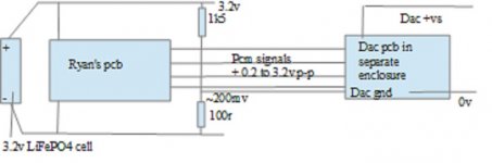
Will this work (raising the output ground by 200mv with a resistor) given that the current consumption is so low?
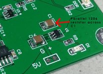
What I meant was parallel a resistor with C1 on my PCB.
Attachments
I asked Ian if I could post this, his reply was from two weeks ago. After repeated emails, and with some initial response, ultimately ending without reply, my suggestion was that I would copy his response, I asked if it were NOT appropriate, that he should let me know - and that never happened. I would invite anyone to check me on that.
Here it is:
"Both bck polarity and the last 1bit LSB are no problem. They just a special case then the waveform in the datasheet. But both of them are within working range. Please see the following technical details.
I have a TDA1541A DAC with FIFOII and PCM board. I did some test again without finding any problem.
So, I did some back review to my old design and TDA1541/A datasheet trying to remember how did I programming the timing of this DAC.
The datasheet shows that both min tHD;DAT and tFBRL can be as short as 0ns. This is exactly the case of my timing, which:
tDH;DATA=0;
tFBRL=0;
tSU;DATA=1/fBCK;
While the timings in TDA1541/A datasheet are:
tDH;DATA=0.5 * 1/fBCK;
tFBRL=0.5 * 1/fBCK;(roughly)
tSU;DATA=0.5 * 1/fBCK;
Timing are within working range in either case, TDA1541/A will work for both.
The only thing is that in my design the LE is one BCK earlier, but this doesn't make LSB being ignored because everything will be included before LE goes low for latches (not register).
Regards,
Ian
-------
I have to say the Ians I2S to PCM board works for me up to 192k with 1541A and without problem, and the best sound I ever had. Just kind of makes me wonder.. and I've had me mate around with his TT and E810F LCR D3a stage, yeah its better.. but not that much better..
Last edited:
I asked Ian if I could post this, his reply was from two weeks ago. After repeated emails without reply, despite my suggestion that I would copy his response, here it is;
Yes, Ian gave me this reply as well and I'm not qualified to comment.
However I did suggest that in simultaneous mode, as there as 16 'spare' clock cycles, is it not possible to delay LE going high for a few cycles so we can see that none of the 16 data clocking cycles occur after it goes high?
I'm waiting to hear from Ian whether my pcm board is repairable after I fed it 15v instead of 5. I may also buy his FifoII board as this supports other input signals than just I2S. When Ryan's board arrives I will use this with a second 1541 dac I will fit into a Sony CDPM18 cd player which is definitely I2S as it uses a TDA1543 dac,
I beg to differ. His assumptions are simply wrong.
Maybe, but how do you explain that many have no issues with 1541 dacs?
Whether audible difference between EC Designs & his are due to 'wrong assumptions' are not proven.
I had no issues with sound quality, indeed, it sounded very engaging until a peak came along and produced the distortion (sounding like sever clipping). But this could be due to the input not being in the correct format, although I can't understand what format would cause it.
I've already provided enough proofs within this thread and I don't really want to waste my time on repeating myself because it leads to nowhere.
For the sake of seeding some doubts within you, lets take a look at his quote:
The only thing is that in my design the LE is one BCK earlier, but this doesn't make LSB being ignored because everything will be included before LE goes low for latches (not register).
He assumes here that TDA1541A latches data on low edge of LE. Can you agree on that with me? If so, take a look at the datasheet of TDA1541:
... The converted samples appear at the output at the positive going transition of the latch enable signal.
So, if converted samples will appear at the positive going transition of LE, at least according to the datasheet, then how, according to you, LSB will appear there as well if it's clocked AFTER LE goes high?
The same goes to assumption regarding BCK, but w/e.
I've already provided enough proofs within this thread and I don't really want to waste my time on repeating myself because it leads to nowhere.
For the sake of seeding some doubts within you, lets take a look at his quote:
He assumes here that TDA1541A latches data on low edge of LE. Can you agree on that with me? If so, take a look at the datasheet of TDA1541:
So, if converted samples will appear at the positive going transition of LE, at least according to the datasheet, then how, according to you, LSB will appear there as well if it's clocked AFTER LE goes high?
The same goes to assumption regarding BCK, but w/e.
I read your & John's comments & I agree with what has been said and it does appear that a mistake has been made and Ian has not read the section on the datasheet relating to simultaneous mode with regards to what LE does. (I have pm'd Ian with links to your replies a couple of weeks ago)
So does this mean that although the lsb is not being clocked in, the rest are clocked and latched okay?
I read your & John's comments & I agree with what has been said and it does appear that a mistake has been made and Ian has not read the section on the datasheet relating to simultaneous mode with regards to what LE does.
So does this mean that although the lsb is not being clocked in, the rest are clocked and latched okay?
In my opinion no. The reason for that is because his converter clocks data on the rising edge of BCK while mine and ecdesigns clocks data on the falling edge according to the datasheet.
Both assumptions are mutually exclusive. The converter either accepts data on rising or falling edge of BCK. It cannot accept data on both rising and falling edge.
If you assume one is correct (clocking data on the falling edge of BCK, like datasheet states and me and ecdesigns have it like that) then the other one (clocking data on the rising edge of BCK, like Ians board does) must be incorrect. You can assume the other way around, but the point still stands, both assumptions are mutually exclusive.
Like many, I have used Ian's PCB with the 1541a for several years. It works and to my ear sounds great at 44k to 192k without issue. But if I understand correctly that does not mean it is as good as it could be. If I am not mistaken, getting 15 bit depth vs 16 does not mean it does not work. It means we are running with a lower signal to noise ratio than the rated performance of the 1541a.
- Home
- Source & Line
- Digital Line Level
- Building the ultimate NOS DAC using TDA1541A