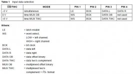
Actually there are three formats: simultaneous, time MUX OB and time MUX TWC.The TDA1541 (A) chip accepts input data in only two formats: OB or TWC. In both formats, the MSB is interpreted as a signed bit.
Attachments
Hi lcsaszar,
Please read to the end of page 4.
Actually there are three formats: simultaneous, time MUX OB and time MUX TWC.
Please read to the end of page 4.
Attachments
Hi SSerg,
Not quite, I use the -most significant- 15 bits for 16 bit resolution and all 16 bits for 17 bit resolution. I also indicated that the full scale current equals 8mA.
When I combine two 16 bit segments I can get 17 bit accuracy, this is how all segmented D/A converters work.
At the zero crossing we get:
1111111111111111 (65535)
While the other channel (segment) is completely turned off (all 16 bits low):
0000000000000000 (0)
So none of the segments is programmed at 32767 (-2mA) at the zero crossing.
The MSB is first sampled (stored) then removed from the code that enters each segment. MSB only governs the data flow into both segments.
Every amplifier-speaker combination distorts quite a lot, then a tiny LSB error becomes irrelevant.
However, among all this distortion, our auditory system remains very picky about zero crossing behaviour (think of audible cross over distortion in push-pull amps). So it still makes a lot of sense (at least to me) to do something about it.
I found time to read the message No. 6116. The idea is good. This is called a segmented DAC.
Indeed, in this way it is possible to significantly reduce the interference from the conversion of the digit / analog near zero.
But to implement the 17-bit DAC on TDA1541 (similar to PCM1704) will not succeed.
The TDA1541 (A) chip accepts input data in only two formats: OB or TWC. In both formats, the MSB is interpreted as a signed bit.
In the PCM1704 chip, the conversion of numbers to the desired format is done inside the chip, and as a result, each of the two internal DACs operates in a dedicated 23-bit segment. Two 23-bit DACs, each working in its 23-bit segment, result in a single 24-bit DAC.
The size of each segment for the TDA1541 pair is 15 bits, since it is impossible to transfer a 16-bit natural number inside the TDA1541 (A) chip, only 15-bit. One bit (MSB) is inevitably spent on the sign of a number. Two DACs, each working on its own 15-bit segment, will result in a single 16-bit DAC.
Not quite, I use the -most significant- 15 bits for 16 bit resolution and all 16 bits for 17 bit resolution. I also indicated that the full scale current equals 8mA.
When I combine two 16 bit segments I can get 17 bit accuracy, this is how all segmented D/A converters work.
At the zero crossing we get:
1111111111111111 (65535)
While the other channel (segment) is completely turned off (all 16 bits low):
0000000000000000 (0)
So none of the segments is programmed at 32767 (-2mA) at the zero crossing.
The MSB is first sampled (stored) then removed from the code that enters each segment. MSB only governs the data flow into both segments.
Every amplifier-speaker combination distorts quite a lot, then a tiny LSB error becomes irrelevant.
However, among all this distortion, our auditory system remains very picky about zero crossing behaviour (think of audible cross over distortion in push-pull amps). So it still makes a lot of sense (at least to me) to do something about it.
Hi John,
PCM1704 forms two 23-bit segments from the input 24-bit code within itself. From the 16-bit code (in the format of OB or TWC), you can form two 15-bit segments.When I combine two 16 bit segments I can get 17 bit accuracy, this is how all segmented D/A converters work.
TDA1541 will accept MSB of the incoming digital word as a sign. If you delete the MSB from the source digital code, the contents of the next bit (the 2nd bit in the source code) will be accepted as a sign.The MSB is first sampled (stored) then removed from the code that enters each segment. MSB only governs the data flow into both segments.
Hi SSerg,
I indicated that I either use the most significant 15 bits of each channel / segment for a 16 bits segmented DAC:
111111111111111-
Or all 16 bits of each channel / segment for a 17 bits segmented DAC:
1111111111111111
Perhaps I was not clear about the fact that I combine L channel (segment #1) and R channel (segment #2) to form one 17 bit mono DAC with one TDA1541A chip. So I need two TDA1541A chips for stereo.
I use a decoder that formats two different data streams, one for each segment. I use TDA1541A simultaneous interface, pin 27 tied to -5V.
Yes, but the related 16 bit L & R channel zero crossing will be shifted 32767 positions away from the newly created signal zero crossing.
This newly created zero crossing is composed of -4mA from one segment, 0mA from the other segment and +4mA from an external bias source, -4 plus 0 plus +4 = 0mA.
With the datasheet application the zero crossing is between these codes:
0111111111111111
1000000000000000
The newly created zero crossing in the segmented version -combines- these codes:
0000000000000000
1111111111111111
These no longer coincide with the actual zero crossing in each 16 bit channel / segment segment.
PCM1704 forms two 23-bit segments from the input 24-bit code within itself. From the 16-bit code (in the format of OB or TWC), you can form two 15-bit segments.
I indicated that I either use the most significant 15 bits of each channel / segment for a 16 bits segmented DAC:
111111111111111-
Or all 16 bits of each channel / segment for a 17 bits segmented DAC:
1111111111111111
Perhaps I was not clear about the fact that I combine L channel (segment #1) and R channel (segment #2) to form one 17 bit mono DAC with one TDA1541A chip. So I need two TDA1541A chips for stereo.
I use a decoder that formats two different data streams, one for each segment. I use TDA1541A simultaneous interface, pin 27 tied to -5V.
TDA1541 will accept MSB of the incoming digital word as a sign. If you delete the MSB from the source digital code, the contents of the next bit (the 2nd bit in the source code) will be accepted as a sign.
Yes, but the related 16 bit L & R channel zero crossing will be shifted 32767 positions away from the newly created signal zero crossing.
This newly created zero crossing is composed of -4mA from one segment, 0mA from the other segment and +4mA from an external bias source, -4 plus 0 plus +4 = 0mA.
With the datasheet application the zero crossing is between these codes:
0111111111111111
1000000000000000
The newly created zero crossing in the segmented version -combines- these codes:
0000000000000000
1111111111111111
These no longer coincide with the actual zero crossing in each 16 bit channel / segment segment.
Hi ec. It looks your circuit forgot to add 1LSB at -1 to +-0 transition.ie,
input 011...1(17bit) converted to 000...0 plus 111...1(16bit)
input 100...0(17bit) converted to 000...0 plus 111...1(16bit) you need 1LSB here as PCM1702/4,
or you can add 1 to the data at the transition and treat wrap around at 111...1 input somehow.(let it clip there it is just a 1LSB short from normal.)
This is little complexed because serial-parallel-serial conversion and a adder are needed so it is better implementing little PLDs.
I also considered sign magnitude with 1541 but not built from my laziness. I will keep eyes on your work.cheers.
edit
The output format is simultaneous then you need to invert MSB for TWC, SSrg mentioned this?I could not understand his post well.
Last edited:
Hi John,
I have no doubt about the possibility and usefulness of creating a segmented DAC based on TDA1541.
I just insist that the resulting segmented DAC will be 16-bit, not 17-bit. The reason is simple: there is nowhere to take a 16-bit mantissa of number. The input signal contains a 15-bit mantissa (15 bits) of sample and a sign (1 bit) of sample. Total 16 bits.
The input signal contains a 15-bit mantissa (15 bits) of sample and a sign (1 bit) of sample. Total 16 bits.
It depends on what player is used. Are there any PC players that would allow adjustment of dither level and wordlenght?
If there aren´t any, maybe a JRiver dither plugin can be created. I would disable JRiver internal dither and use the plugin.
I have looked briefly into creating such a plugin, there´s a software called Flowstone that facilitates development of audio plugins and export as "VST" that can be used in JRiver. IIRC, two independent/uncorrelated random number generators are necessary to make good TPDF dither. I could use one of the provided examples in the Flowstone forum for a random generator, but I´m not sure how to create a second independent generator. I didn´t look at noiseshaped dither yet.
Thanks,
Alex
Hi Alex,
No, it depends primarily on the capabilities of the DAC chip.It depends on what player is used.
SSerg, are you talking about sign magnitude binary code? Indeed, the DAC in discussion is not straight sign magnitude structure but it matters?
For example if we use 4 quadrant multiplying DAC and switch reference polarity with sign bit, it is the sign magnitude, but it must produces massive glitch at zero crossing.Some other circuit can be designed but I think 2DAC(+1LSB) sign magnitude is good choice as PCM63, PCM1702/4 does. Weakness of this configuration is gain matching of upper/lower DACs.
For example if we use 4 quadrant multiplying DAC and switch reference polarity with sign bit, it is the sign magnitude, but it must produces massive glitch at zero crossing.Some other circuit can be designed but I think 2DAC(+1LSB) sign magnitude is good choice as PCM63, PCM1702/4 does. Weakness of this configuration is gain matching of upper/lower DACs.
Last edited:
Hi Shinja,
I'm saying that TDA1541 only accepts data in two formats: OB and TWC. In no other form will you be able to transfer data correctly inside the TDA1541 chip. In both formats, the MSB is interpreted by the chip as a number sign, and 15 bits remain on the mantissa.SSerg, are you talking about sign magnitude binary code?
No, it depends primarily on the capabilities of the DAC chip.
Serg, the input to each channel is still 16 bits of course.
It is the input to the segment logic that can be 17 bits. Like I said it is possible to create a JRiver plugin that will take 24 bits input and add TPDF dither at the desired level. Make the TPDF dither with 2 bits peak to peak amplitude, adjust the level so it lands at bits 16 and 17, and add it. This can be tweaked too. One can experiment with noise shaped dither.
Interface between PC and segment logic still works at 24 bits. It is the job of the segment logic to work only with the 17 most significant bits.
Thanks,
Alex
Hi Alexandre,
The problem is that TDA1541 of each segment will perceive the high bit of this 16-bit segment as a sign. Do you understand? This is how TDA1541 (and TDA1540) is constructed, and it can not be altered. The player here does not help. The problem lies in the hardware.
Sincerely
Serg
The idea is clear. You create two 16-bit segments from a 24-bit signal, and the 17th bit is controlled by an external interface. So?Am I missing something?
The problem is that TDA1541 of each segment will perceive the high bit of this 16-bit segment as a sign. Do you understand? This is how TDA1541 (and TDA1540) is constructed, and it can not be altered. The player here does not help. The problem lies in the hardware.
Sincerely
Serg
The problem is that with TDA1541, you can not form a 16-bit segment (or 16-bit integer number), only 15-bit. Because for the mantissa of number stay only 15 bits.MSB is a sign, so what is the problem here?
The total DAC, which has two 15-bit segments, is equivalent to a 16-bit DAC, but not 17-bit DAC.
Simultaneous Protocol Converter
Hello John,
is it possible that the converter described in post #7078/7079 (timing diagram/schematic) creates a delay of 64 BCK cycles between right and left
channel measured at the output of TDA1541A. With TDA1541A connected to
I2S there is no delay.
Thanks
Hello John,
is it possible that the converter described in post #7078/7079 (timing diagram/schematic) creates a delay of 64 BCK cycles between right and left
channel measured at the output of TDA1541A. With TDA1541A connected to
I2S there is no delay.
Thanks
Just as an information to all the others, COB explained:
http://www.ti.com/lit/an/sbaa042a/sbaa042a.pdf
http://www.ti.com/lit/an/sbaa042a/sbaa042a.pdf
Thank you, useful document.Just as an information ...[/url]
- Home
- Source & Line
- Digital Line Level
- Building the ultimate NOS DAC using TDA1541A