Hi ryanj,
You can find the answer in the TDA1540 datasheet (look at the active divider decoupling cap values).
Yes, it is possible to use following capacitor values:
100uF/25V, 47uF/25V, 22uF/25V, 10uF/25V, 4u7/25V, and 2.2uF/25V. However, we need to identify what bit is on what pin as this is not specified in TDA1541A datasheet and we must be pretty sure before using binary weighted decoupling capacitor values.
The advantage of such arrangement is faster charging of the decoupling caps, and a little bit less space (5mm diameter instead of 6mm diameter for 5 caps). The 25V rating is to lower DC leakage current by staying well away from the rated voltage.
The positive bias current is equal to the TDA1541A negative bias current in order to obtain (almost) zero volts DC on the TDA1541A output when using a passive I/V resistor.
The negative bias current (TDA1541A) equals -2mA / channel. So the positive correction current needs to be approx. the same.
The segmented version has the outputs of L and R channel -connected together- so it requires double positive correction current of +4mA. This is why I use 1K1 bias resistors in the latest schematic. The I/V resistor value is also halved to 75 Ohm as I now have 8mA full scale current.
When running at a 50hz DEM - Would it be possible to use a lower value than 100uF for the LSB ripple filter caps? Theoretically, the LSB would only need only a few uF correct?
You can find the answer in the TDA1540 datasheet (look at the active divider decoupling cap values).
Yes, it is possible to use following capacitor values:
100uF/25V, 47uF/25V, 22uF/25V, 10uF/25V, 4u7/25V, and 2.2uF/25V. However, we need to identify what bit is on what pin as this is not specified in TDA1541A datasheet and we must be pretty sure before using binary weighted decoupling capacitor values.
The advantage of such arrangement is faster charging of the decoupling caps, and a little bit less space (5mm diameter instead of 6mm diameter for 5 caps). The 25V rating is to lower DC leakage current by staying well away from the rated voltage.
For your latest 1541A scheme, you have set up your current bias above the output current of AOL/AOR giving a positive voltage bias on the outputs, have you found any benefits in doing this? I remember you saying a while back that you measured lower distortion when the voltage on the outputs where around -45mV.
The positive bias current is equal to the TDA1541A negative bias current in order to obtain (almost) zero volts DC on the TDA1541A output when using a passive I/V resistor.
The negative bias current (TDA1541A) equals -2mA / channel. So the positive correction current needs to be approx. the same.
The segmented version has the outputs of L and R channel -connected together- so it requires double positive correction current of +4mA. This is why I use 1K1 bias resistors in the latest schematic. The I/V resistor value is also halved to 75 Ohm as I now have 8mA full scale current.
Hi Alexandre,
The whole issue with the DEM clock is that it gets modulated by the input data pattern. So we have a steady clock when no data flows and a frequency modulated clock when data flows. The data pattern frequency modulates the DEM clock. When it gets demodulated the contained data pattern noise is added to the audio signal.
This effect can be greatly reduced by adding two 6K8 bias resistors or one 12K bias resistor. DEM triggering or synchronising would be even better.
In the past I triggered the DEM clock circuit with an external low jitter clock. Grundig did something similar in their CD players so they must have known about this issue too.
But when DEM runs on 50Hz, we no longer have a RF carrier to modulate, so the problem is fixed.
When DEM switches multiple times -within- a sample as is the case with a 250 KHz DEM clock there will be some ground-bounce on the moment of latching. Since 250 KHz DEM is frequency modulated with the data signal there is a risk of adding significant deterministic (data related) jitter by means of induced trigger uncertainty. This is also eliminated with 50 Hz DEM where we only have one DEM bounce every 882 samples.
What about synchronous DEM clock, at a low frequency? One could try 86.13 Hz, 172.26 Hz, 344.53 Hz.
The whole issue with the DEM clock is that it gets modulated by the input data pattern. So we have a steady clock when no data flows and a frequency modulated clock when data flows. The data pattern frequency modulates the DEM clock. When it gets demodulated the contained data pattern noise is added to the audio signal.
This effect can be greatly reduced by adding two 6K8 bias resistors or one 12K bias resistor. DEM triggering or synchronising would be even better.
In the past I triggered the DEM clock circuit with an external low jitter clock. Grundig did something similar in their CD players so they must have known about this issue too.
But when DEM runs on 50Hz, we no longer have a RF carrier to modulate, so the problem is fixed.
When DEM switches multiple times -within- a sample as is the case with a 250 KHz DEM clock there will be some ground-bounce on the moment of latching. Since 250 KHz DEM is frequency modulated with the data signal there is a risk of adding significant deterministic (data related) jitter by means of induced trigger uncertainty. This is also eliminated with 50 Hz DEM where we only have one DEM bounce every 882 samples.
Hi xaled,
Yes of course, 100nF ... 1uF decoupling cap is fine with 250 KHz DEM clock (470 ... 680pF timing cap).
But I experimented with 50Hz DEM clock (1uF timing cap).
This results in much lower ripple frequency (50Hz instead of 250 KHz) so I have to increase the value of the decoupling caps to approx. 100uF/25V (6mm diameter) in order to maintain low ripple current.
Hello John,
perfectly clear, thank you!
greetings,
xaled
Hi SSerg,
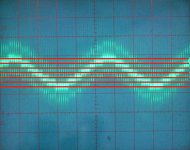
There are only a few bits to reconstruct these very low level signals, then rounding errors will occur. The smaller the signal, the larger the rounding errors.
I have drawn some lines matching the 7 voltage levels that form the -80dB sine wave (or better a coarse approximation of it). I can see no disturbing linearity errors here. The signal passes a pre amp based on a single NJET hybrid semiconductor I developed. (I amplified the voltage across a 75 Ohms passive I/V resistor).
The shape of the signal is dictated by the audio file. It is rounded in a specific way, it could be rounded differently and this may or may not result in a better looking sine wave. But like I said, this is the -80dB signal generated by that test file.
When you look at the -80dB oscillogram (post #6098) from a conventional TDA1541A application with simultaneous interface we can clearly see linearity errors. These no longer occur with the segmented application using the same chip with the same tolerances. Both are running on a 50Hz DEM clock.
I know the difference") . We (my brother and I) performed a one year research project on D/A converter accuracy. I developed hardware (24 bit A/D converter) for very accurate (static) measurements and my brother developed software to analyse the measured data.
. We (my brother and I) performed a one year research project on D/A converter accuracy. I developed hardware (24 bit A/D converter) for very accurate (static) measurements and my brother developed software to analyse the measured data.
It only shows how a D/A converter responds to a 1 KHz signal, seen through an anti aliasing filter and a A/D converter with bit errors that is part of the spectrum analyser.
This tells us little or nothing about how it will sound and IF it is capable of reproducing involving music at all.
Like I mentioned, you need a (large) number of selected recordings to find most of the DAC flaws that only occur when processing complex signals and or very specific data pattern sequences. Sine wave test would not reveal any of these flaws at all. I truly wished these would as this would have saved me years of research.
If things were so simple, every DAC with similar specs (at 1 KHz) would sound -exactly- the same. This is not the case, it is extremely difficult to find two DACs that sound -exactly- the same, even when the DACs are of the same brand, type and batch.
DACs sound different when connected to different bit-perfect digital audio sources and even the applications and OS running on that digital audio source have significant impact on sound.
It is very easy to construct a DAC with good specs, there are hundreds of such DACs available right now, but these usually fail to reproduce music (grainy analytical exaggerated fatiguing sound).
It is close to impossible to construct a DAC that is capable of reproducing really convincing music.
There is a very critical point where sound suddenly turns into involving music that makes your feet tap spontaneously and gives you goose pimps. This difference is only skin deep as maxlorenz once mentioned. That's why it is so incredibly difficult to design and build a DAC that produces music.
It can be seen from them that the 1541 responds confidently to the signal at the level of -80 dB. True, the sinusoid turned into a triangular saw.
There are only a few bits to reconstruct these very low level signals, then rounding errors will occur. The smaller the signal, the larger the rounding errors.
I have drawn some lines matching the 7 voltage levels that form the -80dB sine wave (or better a coarse approximation of it). I can see no disturbing linearity errors here. The signal passes a pre amp based on a single NJET hybrid semiconductor I developed. (I amplified the voltage across a 75 Ohms passive I/V resistor).
The shape of the signal is dictated by the audio file. It is rounded in a specific way, it could be rounded differently and this may or may not result in a better looking sine wave. But like I said, this is the -80dB signal generated by that test file.
When you look at the -80dB oscillogram (post #6098) from a conventional TDA1541A application with simultaneous interface we can clearly see linearity errors. These no longer occur with the segmented application using the same chip with the same tolerances. Both are running on a 50Hz DEM clock.
It seems to me that you confuse two things: the resolving power of conversion and the accuracy of conversion. If the DAC has responded to a weak signal, this does not mean that this response is accurate.
I know the difference
. We (my brother and I) performed a one year research project on D/A converter accuracy. I developed hardware (24 bit A/D converter) for very accurate (static) measurements and my brother developed software to analyse the measured data.The output spectrum makes it possible to give a comprehensive assessment of the quality of the conversion, taking into account various interference and distortions.
It only shows how a D/A converter responds to a 1 KHz signal, seen through an anti aliasing filter and a A/D converter with bit errors that is part of the spectrum analyser.
This tells us little or nothing about how it will sound and IF it is capable of reproducing involving music at all.
Like I mentioned, you need a (large) number of selected recordings to find most of the DAC flaws that only occur when processing complex signals and or very specific data pattern sequences. Sine wave test would not reveal any of these flaws at all. I truly wished these would as this would have saved me years of research.
If things were so simple, every DAC with similar specs (at 1 KHz) would sound -exactly- the same. This is not the case, it is extremely difficult to find two DACs that sound -exactly- the same, even when the DACs are of the same brand, type and batch.
DACs sound different when connected to different bit-perfect digital audio sources and even the applications and OS running on that digital audio source have significant impact on sound.
It is very easy to construct a DAC with good specs, there are hundreds of such DACs available right now, but these usually fail to reproduce music (grainy analytical exaggerated fatiguing sound).
It is close to impossible to construct a DAC that is capable of reproducing really convincing music.
There is a very critical point where sound suddenly turns into involving music that makes your feet tap spontaneously and gives you goose pimps. This difference is only skin deep as maxlorenz once mentioned. That's why it is so incredibly difficult to design and build a DAC that produces music.
Attachments
Even if something inter-modulate, it is no problem when the the product is out of the audio frequency.
For example DEM clock=96kHz and fs=384kHz, when the signal is (the worst case) 20kHz fullscale, first image is at 364kHz.
Thus IMD2 of DEM clock and the signal and the image falls to 76kHz and 268kHz, no problem.The lowest frequency IMD3 is 56kHz, also no problem.
But subjective preference may not match such theory, cleaner HF is why some of us prefer multibit than sigma delta.
Last edited:
I2S-TDA Board
Here is the first draft of the I2S->TDA board based on the John's schema.
I would welcome any feedback and advices on the layot. I'm not a professional pcb designer and this is actually my first board of such complexity.
I'm not particullary happy with the top part of the board but it is the best I can do at the moment.

Thank you,
xaled
Here is the first draft of the I2S->TDA board based on the John's schema.
I would welcome any feedback and advices on the layot. I'm not a professional pcb designer and this is actually my first board of such complexity.
I'm not particullary happy with the top part of the board but it is the best I can do at the moment.
Thank you,
xaled
Last edited:
Hi xaled,
For a first PCB it looks very good. It is good to see that some DIY audio members take the initiative and design and build something.
Don't forget the ground plane.
The most difficult part of PCB routing is component placement. When the components are placed optimally you are already half way. Also place mounting holes before routing, these are often difficult to add after you have completed routing.
With more complex designs it helps to have the majority of traces on the component side running horizontally and have the majority of traces on the solder side running vertically.
You can also swap pins (gate inputs) to simplify routing. This in turn can have an effect on component placement.
Try to avoid running traces underneath decoupling caps. We usually need small (805 size or smaller) caps for effective RF decoupling. These are too small to run a trace between its pads.
Try to route the power supply traces first as these are most important. Think about where the (large) currents flow and what impact this will have on local supply voltages. It would be ideal to run the Vdd supply trace on one side and the Vss return trace on the other side underneath it. This way EM fields cancel and you get far less interference on the board. Again this is not always possible when routing a 2 layer PCB.
Continue with the signal traces. In this specific design the LE signal quality is of utmost importance as it controls sample timing (simultaneous interface). Try to keep it away from noisy signals like data and BCK for example.
After connecting all nets one can try to reduce via count (except for via's that are vital for correct operation). This will force one to reduce lay out to its most effective form.
Hello John,
The current divider in TDA1541 with the DEM generator turned off ensures the accuracy of division at 1-2%. On the oscilloscope screen, you can not see the non-linearity of about 1%, at best at 5-7%, usually at 10%. Therefore, your picture is completely useless for evaluating linearity. The spectral method is much more sensitive.I have drawn some lines matching the 7 voltage levels that form the -80dB sine wave (or better a coarse approximation of it). I can see no disturbing linearity errors here. The signal passes a pre amp based on a single NJET hybrid semiconductor I developed. (I amplified the voltage across a 75 Ohms passive I/V resistor).
In mathematics there is the concept of a necessary and sufficient condition. If even on a sinusoidal signal the spectrum is bad, then on a musical signal everything will be even worse. Therefore, pure spectrum on a sine wave test signal is a necessary condition, but not sufficient. Therefore, analysis of the spectra must be supplemented by listening to phonograms. But to achieve pure spectrum on a sinusoid all the same it is necessary.This tells us little or nothing about how it will sound...
Well said, Master.
Dear SSerg said:
Unfortunately, we cannot take any knowledge as granted truth.
We must question every pre-conception in order to achieve the goal of perfect musical reproduction.
The old masters called this "methodical doubt".
Lowest THD is not necesarily giving us good sounding gear. One of the first proves we had on this thread was John's introduction of the diffamp instead of the last opamp of the cascade in the output of the DI16 DIDAC. A small discrete differential amplifier with plenty of resistors as CCS and passive loading but that sounds much more involving and true to music than the best opamp I had then, though it has not so good specs...now I took the liberty of modifying it to get a low thermal memory diffamp (in the future with cascoded JFET buffer) that sounds even better IMHO.
Cheers,
M.
Dear SSerg said:
Classical I/U cascade on the opamp (AD842);
Unfortunately, we cannot take any knowledge as granted truth.
We must question every pre-conception in order to achieve the goal of perfect musical reproduction.
The old masters called this "methodical doubt".
Lowest THD is not necesarily giving us good sounding gear. One of the first proves we had on this thread was John's introduction of the diffamp instead of the last opamp of the cascade in the output of the DI16 DIDAC. A small discrete differential amplifier with plenty of resistors as CCS and passive loading but that sounds much more involving and true to music than the best opamp I had then, though it has not so good specs...now I took the liberty
of modifying it to get a low thermal memory diffamp (in the future with cascoded JFET buffer) that sounds even better IMHO. Cheers,
M.
Hi maxlorenz,
I did not say that the Op-Am gives a better sound. Our dispute about the other: the frequency of the DEM generator affects the linearity of the TDA1541 or not. In my opinion, there is influence. And to make sure of this, it is necessary to study the spectra for different DEM frequencies: for the nominal frequency 200 kHz, and 50 Hz, and 500-800 kHz. For this, the I / U cascade on the op-amp is quite suitable.
I did not say that the Op-Am gives a better sound. Our dispute about the other: the frequency of the DEM generator affects the linearity of the TDA1541 or not. In my opinion, there is influence. And to make sure of this, it is necessary to study the spectra for different DEM frequencies: for the nominal frequency 200 kHz, and 50 Hz, and 500-800 kHz. For this, the I / U cascade on the op-amp is quite suitable.
Hi maxlorenz,
I did not say that the Op-Am gives a better sound. Our dispute about the other: the frequency of the DEM generator affects the linearity of the TDA1541 or not. In my opinion, there is influence. And to make sure of this, it is necessary to study the spectra for different DEM frequencies: for the nominal frequency 200 kHz, and 50 Hz, and 500-800 kHz. For this, the I / U cascade on the op-amp is quite suitable.
Yes, I understood this. You are way more knowledgeable than I am, I know this. I was not clear in my post that it was not addressed to you: I only wanted to point out this to the rest of the mates that still use convenience solutions instead of discrete and modifiable subcircuits to experiment better ways of musical reproduction.
My present experiments with low TMD circuits opened my eyes again...
Cheers,
M.
I was not clear in my post that it was not addressed to you.
OK
Hi xaled,
For a first PCB it looks very good. It is good to see that some DIY audio members take the initiative and design and build something.
Don't forget the ground plane.
Thank you for the compliment. It is nice to know that even the initial draft is not so bad
.I updated the board as far as I could according to your comments. Ground plane was there already, but it did not show up for some reason in the first picture.

I would appreciate any further comments that would help improve the board.

Would Guido Tent's recommendations on the subject of PS chip decoupling be useful in this case?
Best wishes,
M.
Attachments
4000 series shift registers
Hi zoran,
No it's way too slow (propagation delay) to ensure correct operation even at 44.1 KHz while using 5V supply voltage.
The decoder needs to run on 2V4 ... 3V3 supply voltage for low noise.
If you don't like 4 shift registers and only need 16 bit resolution (17 bit with segmented TDA1541A application), it is possible to use clock stopping on the delay shift register.
This way the number of shift registers can be halved while still offering required 32 bit delay (16 bit real data bit delay plus 16 bit paused delay).
We stop the shift register when the bits we don't use / need pass by. These bits do not get clocked in (skipped) when the clock stops, so only the 16 bits we are interested in are temporarily stored in the register.
The delay can be configured for 17 or 24 bit resolution. For 24 bit resolution we need 3 shift registers, for 17 bits only 2 (16 bit data delay and MSB pre-fetch outside the shift register delay circuit).
So we have MSB + 16 bits (2 x 74LV164 delay) = 17 bits.
Or MSB + 24 bits (3 x 74LV164 delay) = 25 bits.
We can use the Q4 counter output (74HC4060) for creating required 16 bit clock burst signal for the shift registers. Invert Q4 (74LVC04) and combine the inverted Q4 output with BCK using an AND gate (74LVC08).
If we need a 24 bit clock burst signal we also have to include the Q3 signal for the decoder.
NOR gate (74LVC02) with Q4 and Q3 outputs connected to its inputs. And gate combines NOR gate output with BCK.
Hi zoran,
Can we use some 1x32bit shift register for instance HEF4557B against 4 x 8bit hc164 if the speed and max F are OK?
No it's way too slow (propagation delay) to ensure correct operation even at 44.1 KHz while using 5V supply voltage.
The decoder needs to run on 2V4 ... 3V3 supply voltage for low noise.
If you don't like 4 shift registers and only need 16 bit resolution (17 bit with segmented TDA1541A application), it is possible to use clock stopping on the delay shift register.
This way the number of shift registers can be halved while still offering required 32 bit delay (16 bit real data bit delay plus 16 bit paused delay).
We stop the shift register when the bits we don't use / need pass by. These bits do not get clocked in (skipped) when the clock stops, so only the 16 bits we are interested in are temporarily stored in the register.
The delay can be configured for 17 or 24 bit resolution. For 24 bit resolution we need 3 shift registers, for 17 bits only 2 (16 bit data delay and MSB pre-fetch outside the shift register delay circuit).
So we have MSB + 16 bits (2 x 74LV164 delay) = 17 bits.
Or MSB + 24 bits (3 x 74LV164 delay) = 25 bits.
We can use the Q4 counter output (74HC4060) for creating required 16 bit clock burst signal for the shift registers. Invert Q4 (74LVC04) and combine the inverted Q4 output with BCK using an AND gate (74LVC08).
If we need a 24 bit clock burst signal we also have to include the Q3 signal for the decoder.
NOR gate (74LVC02) with Q4 and Q3 outputs connected to its inputs. And gate combines NOR gate output with BCK.
Hi maxlorenz,
This decoder circuit only needs to handle data. So all we are interested in here is data integrity and that can even be guaranteed with a single decoupling cap (I tested the air wire setup this way).
I use low supply voltage (2V4 ... 3V3) and 1K resistors on the data and bit clock outputs so noise injection (related to fast rising and falling transients) stays low.
The critical signal for timing (if that matters) bypasses the whole circuit and goes straight to the LE sample timing input (TDA1541A in simultaneous mode).
For the USB receiver, decoupling is extremely important, think of noise on the analogue PLL supply.
Decoupling caps also provide more energy for producing more interference. Compare this with short circuiting a 10,000uf cap charged to 63V vs no cap. The higher the peak currents (local charged decoupling cap), the higher the interference. So one has to find a compromise between local supply rail quality (for reliable logic levels) and interference power. It may even be desired to add low Ohmic series resistors to each decoupling cap. This limits local peak switching currents and lowers the Q factor of LC resonance circuits that will always be formed.
Decoupling LC series resonant circuits could make matters worse depending on tuning frequency and target frequency that needs to be attenuated. If such LC resonance is unwanted we need to get LC circuit Q factor down using series or shunt resistors (shunt regulator) for example.
Every single capacitor is basically a LC series resonance circuit that will resonate at a specific frequency. Suppliers often include graphs that show a V curve where impedance drops to the resonance frequency, then rises again (less effective decoupling at these higher frequencies).
When we want to effectively suppress one specific frequency (say 2.8224 MHz bit clock noise) we could create a tuned LC circuit using PCB trace plus decoupling cap inductance plus pure capacitance to resonate at exactly 2.8224 MHz. This would be more effective that simply adding 100nF caps to the board.
Suppose we have total trace inductance (decoupling loop) of say 12nH:
Calculator for the Inductance of a Flat Wire
And we need to tune the decoupling circuit on 2.8224 MHz then we can use this LC calculator:
Resonant Frequency Calculator
We get a pure capacitance of 265nF.
So we could get more effective decoupling by using say 270nF decoupling cap here.
the "standard" 100nF would resonate at 4.59 Mhz and would not be very effective here.
We can also deliberately introduce multiple resonance dips (using different decoupling cap values in combination with trace length) that cover a large bandwidth. This way we can have much more effective decoupling over a much larger bandwidth then simply adding 100nF caps in parallel with each chip.
In the decoder circuit we can have dominant frequencies at 2.8224 MHz, 3.072 MHz, 5.6448 MHz, and 6.144 MHz that we could tackle with tuned decoupling circuits.
Would Guido Tent's recommendations on the subject of PS chip decoupling be useful in this case?
This decoder circuit only needs to handle data. So all we are interested in here is data integrity and that can even be guaranteed with a single decoupling cap (I tested the air wire setup this way).
I use low supply voltage (2V4 ... 3V3) and 1K resistors on the data and bit clock outputs so noise injection (related to fast rising and falling transients) stays low.
The critical signal for timing (if that matters) bypasses the whole circuit and goes straight to the LE sample timing input (TDA1541A in simultaneous mode).
For the USB receiver, decoupling is extremely important, think of noise on the analogue PLL supply.
Decoupling caps also provide more energy for producing more interference. Compare this with short circuiting a 10,000uf cap charged to 63V vs no cap. The higher the peak currents (local charged decoupling cap), the higher the interference. So one has to find a compromise between local supply rail quality (for reliable logic levels) and interference power. It may even be desired to add low Ohmic series resistors to each decoupling cap. This limits local peak switching currents and lowers the Q factor of LC resonance circuits that will always be formed.
Decoupling LC series resonant circuits could make matters worse depending on tuning frequency and target frequency that needs to be attenuated. If such LC resonance is unwanted we need to get LC circuit Q factor down using series or shunt resistors (shunt regulator) for example.
Every single capacitor is basically a LC series resonance circuit that will resonate at a specific frequency. Suppliers often include graphs that show a V curve where impedance drops to the resonance frequency, then rises again (less effective decoupling at these higher frequencies).
When we want to effectively suppress one specific frequency (say 2.8224 MHz bit clock noise) we could create a tuned LC circuit using PCB trace plus decoupling cap inductance plus pure capacitance to resonate at exactly 2.8224 MHz. This would be more effective that simply adding 100nF caps to the board.
Suppose we have total trace inductance (decoupling loop) of say 12nH:
Calculator for the Inductance of a Flat Wire
And we need to tune the decoupling circuit on 2.8224 MHz then we can use this LC calculator:
Resonant Frequency Calculator
We get a pure capacitance of 265nF.
So we could get more effective decoupling by using say 270nF decoupling cap here.
the "standard" 100nF would resonate at 4.59 Mhz and would not be very effective here.
We can also deliberately introduce multiple resonance dips (using different decoupling cap values in combination with trace length) that cover a large bandwidth. This way we can have much more effective decoupling over a much larger bandwidth then simply adding 100nF caps in parallel with each chip.
In the decoder circuit we can have dominant frequencies at 2.8224 MHz, 3.072 MHz, 5.6448 MHz, and 6.144 MHz that we could tackle with tuned decoupling circuits.
Hi maxlorenz,
This decoder circuit only needs to handle data. So all we are interested in here is data integrity and that can even be guaranteed with a single decoupling cap (I tested the air wire setup this way).
For the USB receiver, decoupling is extremely important, think of noise on the analogue PLL supply.
Decoupling LC series resonant circuits could make matters worse depending on tuning frequency and target frequency that needs to be attenuated. If such LC resonance is unwanted we need to get LC circuit Q factor down using series or shunt resistors (shunt regulator) for example.
Every single capacitor is basically a LC series resonance circuit that will resonate at a specific frequency. Suppliers often include graphs that show a V curve where impedance drops to the resonance frequency, then rises again (less effective decoupling at these higher frequencies).
We can also deliberately introduce multiple resonance dips (using different decoupling cap values in combination with trace length) that cover a large bandwidth. This way we can have much more effective decoupling over a much larger bandwidth then simply adding 100nF caps in parallel with each chip.
In the decoder circuit we can have dominant frequencies at 2.8224 MHz, 3.072 MHz, 5.6448 MHz, and 6.144 MHz that we could tackle with tuned decoupling circuits.
Thanks -EC- for that very interesting input.
Reality is like an onion: when you are perfectly happy with the outer coat, you realize that there is always one other, deeper coat under it...
Cheers,
M.
Some examples of signed magnitude D/A converters are the Soekris DAC and the PCM1704 just to name a few of many.
...We end up with a 17 bit dual mono TDA1541A signed magnitude DAC, full scale current doubles to 8mA and resolution is doubled to 17 bits.
Hi John,
I found time to read the message No. 6116. The idea is good. This is called a segmented DAC.
Indeed, in this way it is possible to significantly reduce the interference from the conversion of the digit / analog near zero.
But to implement the 17-bit DAC on TDA1541 (similar to PCM1704) will not succeed.
The TDA1541 (A) chip accepts input data in only two formats: OB or TWC. In both formats, the MSB is interpreted as a signed bit.
In the PCM1704 chip, the conversion of numbers to the desired format is done inside the chip, and as a result, each of the two internal DACs operates in a dedicated 23-bit segment. Two 23-bit DACs, each working in its 23-bit segment, result in a single 24-bit DAC.
The size of each segment for the TDA1541 pair is 15 bits, since it is impossible to transfer a 16-bit natural number inside the TDA1541 (A) chip, only 15-bit. One bit (MSB) is inevitably spent on the sign of a number. Two DACs, each working on its own 15-bit segment, will result in a single 16-bit DAC.
Sincerely,
Serg
- Home
- Source & Line
- Digital Line Level
- Building the ultimate NOS DAC using TDA1541A