Sorry for off topic, but what interested me is that you are trying with great efforts to get rid of pcb micro-noises and such things that certainly exist in capacitors receiving AC.
Oil is very impracticalfor you pcb dac because I don't think it will help with vibrations. And it will stop the air flow and provide thermal isolation for your components which you agree should be avoided.
Hey maxlorenz, waxes could be good if they transfer heat and are rigid enough and melting point is way over the components temperature. It could be a research subject. Both waxes and most epoxy can be removed with re-heating and special solvents but it is not an interesting job.
for epoxy a simple search led me to great products:
you should read that website to learn better than my poor english allows") Epoxy Resin Varnishes | Encapsulants for Transformers | Electronic Sensor Encapsulant | Epoxy Resin Potting Compound | Transformer Potting | Epic Resins - Manufacturer of Epoxy Resins and Polyurethane Compounds
Epoxy Resin Varnishes | Encapsulants for Transformers | Electronic Sensor Encapsulant | Epoxy Resin Potting Compound | Transformer Potting | Epic Resins - Manufacturer of Epoxy Resins and Polyurethane Compounds
epoxy able industrial applications machinery for the ambitious diy audiophile :
other benefits of encapsulation : Meter Mix Dispense Systems for Adhesives and Sealants by Sealant Equipment & Engineering
Oil is very impracticalfor you pcb dac because I don't think it will help with vibrations. And it will stop the air flow and provide thermal isolation for your components which you agree should be avoided.
Hey maxlorenz, waxes could be good if they transfer heat and are rigid enough and melting point is way over the components temperature. It could be a research subject. Both waxes and most epoxy can be removed with re-heating and special solvents but it is not an interesting job.
for epoxy a simple search led me to great products:
you should read that website to learn better than my poor english allows
Epoxy Resin Varnishes | Encapsulants for Transformers | Electronic Sensor Encapsulant | Epoxy Resin Potting Compound | Transformer Potting | Epic Resins - Manufacturer of Epoxy Resins and Polyurethane Compoundsepoxy able industrial applications machinery for the ambitious diy audiophile :
An externally hosted image should be here but it was not working when we last tested it.
other benefits of encapsulation : Meter Mix Dispense Systems for Adhesives and Sealants by Sealant Equipment & Engineering
If anyone is keen to experiment with micro-dampening strategies for components on PCB's may I suggest:
1. use mineral oil as its
2. Place the PCB in the bottom of a moulded alloy case with connectors on the top of the rear side above the oil level to prevent direct leaks and so the connectors prevent oil wicking up the cables. The aluminium box will allow passive cooling via air convection and by radiation from the external surface

3. Listen with a group and measure using air first and then poor in the oil while its still playing and listen for any changes and re-measure
1. use mineral oil as its
- cheap,
- easily available,
- reversible,
- able to cool via passive convection flow like air
- arguably five times better for convection cooling then air so may moderate local hot spots eg the actual TDA1541a chip itself
- already used in transformer cooling and computer cooling (http://www.pugetsystems.com/submerged.php)
- over 600 times denser then air so should dampen micro-resonance accelerations by over 600 times compared to air
- good dielectric at 2.3
2. Place the PCB in the bottom of a moulded alloy case with connectors on the top of the rear side above the oil level to prevent direct leaks and so the connectors prevent oil wicking up the cables. The aluminium box will allow passive cooling via air convection and by radiation from the external surface
3. Listen with a group and measure using air first and then poor in the oil while its still playing and listen for any changes and re-measure
Last edited:
If anyone is keen to experiment with micro-dampening strategies for components on PCB's may I suggest:
1. use mineral oil as its
- cheap,
- easily available,
- reversible,
- able to cool via passive convection flow like air
- arguably five times better for convection cooling then air so may moderate local hot spots eg the actual TDA1541a chip itself
- already used in transformer cooling and computer cooling (Custom PC; Mineral Oil Submerged Computer)
- over 600 times denser then air so should dampen micro-resonance accelerations by over 600 times compared to air
- good dielectric at 2.3
2. Place the PCB in the bottom of a moulded alloy case with connectors on the top of the rear side above the oil level to prevent direct leaks and so the connectors prevent oil wicking up the cables. The aluminium box will allow passive cooling via air convection and by radiation from the external surface
3. Listen with a group and measure using air first and then poor in the oil while its still playing and listen for any changes and re-measure
Cool.
Thanks.
First I have to get a definitive version of my DAC.
M.
Wheat flour is 2x mineral oil thermal conductivity, for a 'tasty' sound. In an enclosed recipient the heat transfer might even be less than letting the components in free circulating air. I remember seeing that computer in the oil with the difference that a pump was circulating the oil to a radiator.
Even better is plasticine, 4x conduction of oil, it is easy to apply by warming it up first. I would fear for oil spills or catching on fire...
electronic grade Epoxy is rated 2.16 W/mK and mineral oil is 0.16 W/mk, air 0.02, Paraffin Wax 0.25 , wheat flour 0.45!
Even better is plasticine, 4x conduction of oil, it is easy to apply by warming it up first. I would fear for oil spills or catching on fire...
electronic grade Epoxy is rated 2.16 W/mK and mineral oil is 0.16 W/mk, air 0.02, Paraffin Wax 0.25 , wheat flour 0.45!
Last edited:
Sand and Mounting Putty
All of this discussion about mineral oil got me experimenting.
I put some mounting putty right on the clocks. A nice big blob squashed into place. Then followed that with my traditional dry sand in zip locked bags laid in around the various PCBs of my DAC.
No question as good as a clock upgrade. Thanks for the inspiration.
All of this discussion about mineral oil got me experimenting.
I put some mounting putty right on the clocks. A nice big blob squashed into place. Then followed that with my traditional dry sand in zip locked bags laid in around the various PCBs of my DAC.
No question as good as a clock upgrade.
Thanks for the inspiration.I put some mounting putty right on the clocks...
No question as good as a clock upgrade.
Is mounting putty a sort of mastic?
I once transformed an cheap Sony DVD into a half decent transport with lots of mastic damping... I think it is somewhere out there ...
Cheers,
M.
Hi M.
The stuff I used was from my local office supply. See link from Amazon. Blue tack and others likely work as well. Like modeling clay but not oily.
http://www.amazon.ca/Scotch-Adhesive-Putty-Removable-860/dp/B000AN7EW4
Combined with a BG N on the power pin of the clock, a game changer.
Walter
The stuff I used was from my local office supply. See link from Amazon. Blue tack and others likely work as well. Like modeling clay but not oily.
http://www.amazon.ca/Scotch-Adhesive-Putty-Removable-860/dp/B000AN7EW4
Combined with a BG N on the power pin of the clock, a game changer.
Walter
TDA1541 (non-A) : external SCK (mclk) needed ?
Hi fellows,
Re reading the TDA151 non-A datasheet, I asking myself if this chip can be working only with a SCK external signal on pin 4 when connected in true I2S mode... so forbiding the possibility to use it seriously in simultaneous mode ?
The internal dem time cap has an average 200 Khz (between 150 and 250 K hz on the Philips datasheet !), what is the advised value of 14 DEM caps witrh such timing ? 0.1 uF max ?
Thanks,
I made some test with tda1541 non-A in simultaneous mode and it dorsn't rock like Lampizator wrote, dspite the better 0.5 LSB precision of the non A in relation to the newer TDA1541A !
Any thought ?
Hi fellows,
Re reading the TDA151 non-A datasheet, I asking myself if this chip can be working only with a SCK external signal on pin 4 when connected in true I2S mode... so forbiding the possibility to use it seriously in simultaneous mode ?
The internal dem time cap has an average 200 Khz (between 150 and 250 K hz
on the Philips datasheet !), what is the advised value of 14 DEM caps witrh such timing ? 0.1 uF max ?Thanks,
I made some test with tda1541 non-A in simultaneous mode and it dorsn't rock like Lampizator wrote, dspite the better 0.5 LSB precision of the non A in relation to the newer TDA1541A !
Any thought ?
Scope shots
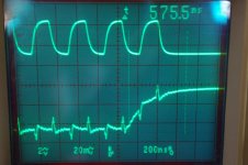
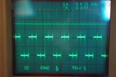
Hi Fellas,
Dont mean to litter the forum with scope shots, but just wondering what exactly is going on here (aside from the noise from BCK on the Analog outputs) It looks like the sample starts before the least significant bit is clocked in? According to the data sheet (TDA1541A) this shouldn't be so - Unless i'm not clear about something.
Also notice how much BCK is visible on the Analog outputs without I2S attenuation - Hope to change that soon.
Bandwidth limited,
Top trace is BCK using only 50mhz probe - hence the slow rise time.
Bottom trace 11025hz square wave at full scale current output.
Simultaneous mode.
Ryan
Attachments
Last edited:
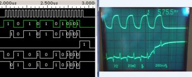
Hi Guys,
Seems offset binary format works a bit different than time multiplexed mode. The sample is triggered on the positive going edge of LE - latch enable. Ian Canada has provided some logic analysis of what his PCB is doing. Looks like my scope shot shows what should be expected. Nothing to worry about.
Image to the left:
BCK
DATA L
DATA R
LE
DATA L inverted
DATA R inverted
Image on the right:
BCK
Analog output - 11025hz square (corresponds with LE on the analysis)
Attachments
Last edited:
Hi John,
In the PCB Ryan uses and we "developed"by copying your design with your benediction and what you given to the DIY communauty, I believe an error was made by us but hope this is not important as Ryan says...
I permitt to ask you as you are our main inspiration source with P. Rogic and T. Loesch threads on the different forums.
Here is the problem (hope not !) : the pcb we use have a top AND bottom digital ground where all the decoupling supply are tied on those two continuous digital ground. Both side of pin 14 (DGND) is tied on those digital ground plane and only the upper side of pin 5 (AGND), so here pin 5 & pin 14 are tied together on te upper side.
We went for your central analog starground on the bottom side (so tied to pin 5 and not communicated with the bottom digital ground around it on the bottom face but only with the upper side by the pin 5.
But -15 V have two decoupling grounds :
- its direct path to pin 5 (so one of the analog path of the analog starground between the DEM caps grounds) for a little value for smt cap (the // value of the main radial cap)
- a local decoupling via tied on the two sides of the digital ground at small distance of the pin 14 which is itself tied on the two sides of the digital ground !
Doest it make sense than the main cap has a close reference to pin 14 and at the same time its // decoupling cap of a smaller value for higher frequencies is tied directly to pin 5 by a separate path ! Is it not better than the decoupling cap to be near of the main cap with a perfect same ground reference for digital stuffs ?
May you please help us, I know we ask you a lot but as you inspired us for this design I would like to avoid any major problem by using this board (100 units were gently print for the communauty by Ryan who was the drawer).
A simple and short answer could be great enough :
For the -15V local decoupling cap use the analog ground path only or the digital ground only or OK, no major problem to use both ways at the same time (even if pin 14 is far from the analog ground reference (pin5) with the main cap tied at the digital ground near pin 14 and the little smt decoupling cap tied near pin 5 (direct path).
I believe what Ryan is doing to acheive above is interresting but I wouldn't it is on a too bad layout, so if we, he, print a V2 board, your advice about what I ask could be of a major interrest (or not if this is not important);
regards
Last edited:
...the pcb we use have a top AND bottom digital ground where all the decoupling supply are tied on those two continuous digital ground. Both side of pin 14 (DGND) is tied on those digital ground plane and only the upper side of pin 5 (AGND), so here pin 5 & pin 14 are tied together on te upper side.
PCBs have been received!
-Electroless nickel/immersion gold plating
You diyAudiophiles have strange priorities. Best practice calls for a single, uninterrupted, dedicated ground plane. But rather than paying a little extra for a 4-layer PCB, you happily pay extra for gold plated traces, which does nothing for signal integrity. "Oh, yeah? But gold plated traces look so cool. Who cares about the sound quality?" With audiophiles, bling trumps all.
Eldamo, i personally connot see any of your input in ryans board, i heard his previous one which was excellent. He made the changes himself, before bringing out the current board. I dont think this warrants you saying that ''we developed it'', when clearly ryan j was the only one who made it.
- Home
- Source & Line
- Digital Line Level
- Building the ultimate NOS DAC using TDA1541A