hi youknowyou,
USB cables like all other interlinks will filter / change the source frequency spectrum. Even cables of the same brand and type can have different properties as it is impossible to make two exactly identical cables.
These marginal differences may be audible in a double blind test depending on the resolution of the connected audio set.
Source interference changes the sound through related jitter spectrum, I2S signals and power supply / ground circuits.
The XTOS Toslink output eliminates (HF) interference that enters by ground-loops and it bandlimits the received source spectrum to approx. 13 MHz instead of a few GHz with a direct USB connection. The interference from such limited bandwidth signal is easier to attenuate.
I use good quality USB cables, these should cost no more than approx. $10.
I do not use the crystal oscillators in the XTOS to directly clock the DAC. Toslink will add more jitter so the clocks and power supply in the XTOS are not critical.
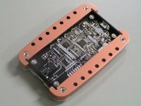
I attached a photograph of the XTOS prototype. It supports 44.1/16 ... 192/24.
It is USB powered and connection is made through a micro USB socket. I use a SMPS 1V core voltage regulator (in order to minimise USB bus current) and a 3V3 LDO plus dedicated power supply monitor and reset circuits.
The small chip close to the USB socket is a USB to parallel converter, the PHY. It contains on-chip voltage regulators. This is a new version of the PHY where the bias voltage issue is fixed.
The large chip is the XMOS multicore (state machine) processor.
There are 3 low jitter Epson miniature crystal oscillators for 26 MHz PHY & XMOS clock, 22.579 and 24.576 MHz audio clocks. These oscillators are powered by a low noise LDO voltage regulator.
The Toslink output signal generated by the XMOS processor is synchronously reclocked by one of the audio clocks (depends on selected sample rate) in order to ensure low jitter. I use an ultra high speed D flip flop for reclocking.
There are 4 indicator LEDs for USB connection, streaming, 16/24 bit and bit-perfect test.
The bit perfect test requires a test track with a sawtooth signal on it. This audio file is automatically detected and it initiates the bit-perfect test. The bit-perfect test can be initiated at any time during listening, it is not necessary to put the XTOS in a test mode.
The XTOS works without drivers when the source supports UAC1 or UAC2. Jumper setting on the XTOS can force the XTOS to power up in UAC1 or UAC2 mode. If one uses Windows and wants to use sample rate higher than 96 KHz a driver is needed, the Thesycon driver for example. In this case one has to check various settings in order to achieve bit-perfect playback. Mac and Linux support UAC2 and work without drivers.
The XTOS firmware can be updated through USB when required.
These products are fully handcrafted, the PCB is exposed, developed, etched, tinned and drilled in house. The via's consist of solid copper wire and are riveted into the PCB by hand. The parts are soldered on the PCB by hand in order to minimise thermal stress and ensure long service life. The PCB is routed single-sided (like all my new designs). The other side of the PCB contains a solid ground plane. Wire bridges are made of tinned copper wire with PTFE (Teflon) insulation.
hi ecdesigns, Do you feel that different usb cable, that connect the computer to the XTOS, can make a difference to SQ or any usb cable work exactly the same?
USB cables like all other interlinks will filter / change the source frequency spectrum. Even cables of the same brand and type can have different properties as it is impossible to make two exactly identical cables.
These marginal differences may be audible in a double blind test depending on the resolution of the connected audio set.
Source interference changes the sound through related jitter spectrum, I2S signals and power supply / ground circuits.
The XTOS Toslink output eliminates (HF) interference that enters by ground-loops and it bandlimits the received source spectrum to approx. 13 MHz instead of a few GHz with a direct USB connection. The interference from such limited bandwidth signal is easier to attenuate.
I use good quality USB cables, these should cost no more than approx. $10.
About the XTOS, I see you use the Xmos chip. do you use the Cyrstek CCHD-957 clocks? what is the regulation used: double power regulation?
I do not use the crystal oscillators in the XTOS to directly clock the DAC. Toslink will add more jitter so the clocks and power supply in the XTOS are not critical.
can we have more information about the XTOS design and maybe pictures?
I attached a photograph of the XTOS prototype. It supports 44.1/16 ... 192/24.
It is USB powered and connection is made through a micro USB socket. I use a SMPS 1V core voltage regulator (in order to minimise USB bus current) and a 3V3 LDO plus dedicated power supply monitor and reset circuits.
The small chip close to the USB socket is a USB to parallel converter, the PHY. It contains on-chip voltage regulators. This is a new version of the PHY where the bias voltage issue is fixed.
The large chip is the XMOS multicore (state machine) processor.
There are 3 low jitter Epson miniature crystal oscillators for 26 MHz PHY & XMOS clock, 22.579 and 24.576 MHz audio clocks. These oscillators are powered by a low noise LDO voltage regulator.
The Toslink output signal generated by the XMOS processor is synchronously reclocked by one of the audio clocks (depends on selected sample rate) in order to ensure low jitter. I use an ultra high speed D flip flop for reclocking.
There are 4 indicator LEDs for USB connection, streaming, 16/24 bit and bit-perfect test.
The bit perfect test requires a test track with a sawtooth signal on it. This audio file is automatically detected and it initiates the bit-perfect test. The bit-perfect test can be initiated at any time during listening, it is not necessary to put the XTOS in a test mode.
The XTOS works without drivers when the source supports UAC1 or UAC2. Jumper setting on the XTOS can force the XTOS to power up in UAC1 or UAC2 mode. If one uses Windows and wants to use sample rate higher than 96 KHz a driver is needed, the Thesycon driver for example. In this case one has to check various settings in order to achieve bit-perfect playback. Mac and Linux support UAC2 and work without drivers.
The XTOS firmware can be updated through USB when required.
These products are fully handcrafted, the PCB is exposed, developed, etched, tinned and drilled in house. The via's consist of solid copper wire and are riveted into the PCB by hand. The parts are soldered on the PCB by hand in order to minimise thermal stress and ensure long service life. The PCB is routed single-sided (like all my new designs). The other side of the PCB contains a solid ground plane. Wire bridges are made of tinned copper wire with PTFE (Teflon) insulation.
Attachments
These products are fully handcrafted, the PCB is exposed, developed, etched, tinned and drilled in house. The via's consist of solid copper wire and are riveted into the PCB by hand. The parts are soldered on the PCB by hand in order to minimise thermal stress and ensure long service life. The PCB is routed single-sided (like all my new designs). The other side of the PCB contains a solid ground plane. Wire bridges are made of tinned copper wire with PTFE (Teflon) insulation.
Wow. Do you have nanobots working for you?

I would have used silver wire bridges, instead
Very impressive work.
M.

The Xmos I2S would replace the CS8412, so the CS8412 should be removed. The Xmos I2S output should be connected to the TDA1541A as follows:
- LRCK out to TDA1541 pin 1
- BCLK out to TDA1541 pin 2 (pin 2 stays connected to pin 4)
- DATA out to TDA1541 pin 3
- Ground out to TDA1541 Ground
- LRCK out to TDA1541 pin 1
- BCLK out to TDA1541 pin 2 (pin 2 stays connected to pin 4)
- DATA out to TDA1541 pin 3
- Ground out to TDA1541 Ground
Last edited:
The Xmos I2S would replace the CS8412, so the CS8412 should be removed. The Xmos I2S output should be connected to the TDA1541A as follows:
- LRCK out to TDA1541 pin 1
- BCLK out to TDA1541 pin 2 (pin 2 stays connected to pin 4)
- DATA out to TDA1541 pin 3
- Ground out to TDA1541 Ground
hi,
thank you for your information..
if i had to remove CS8412, then i can't use my CDP again (it only have optical and spdif digital out)..
another alternative is to use async USB receiver with spdif output, will this degrade the quality of digital data ?
thanks
You can always rip your compact discs to memory and do away with your cd player.
The CS8412 has high jitter so leaving it in place would be less than optimal. USB to SPDIF would allow you to have an USB connection to your dac though if you keep the CS8412.
Proper integration of the Xmos I2S to the dac is also important. I2S lines between the Xmos and TDA need to be kept short as possible (less than 100mm but even shorter is better) and proper terminations and grounding scheme is critical in getting the best out of the Xmos usb.
So a poorly implemented usb to I2S solution may not beat a well done SPDIF setup.
hi ecdesign,
it seem the ultimate nos dac is ended with MK7, is it correct?
about the 1uf decoupling caps, i can not found the film smd cornel dubilier.
is it possible to use 1uf 16v tantalum smd caps for those positions?
with all positive tantalum goes to the ground plane.
how it will affect the sound?
thanks.
Peter
- Passive masterclock that completely eliminates power supply related phase noise.
John,
Passive clock??
I recall you mentioning that your master clock somehow makes use of fuzzy logic technology. Can you elaborate a bit?
Also, whether the clock is passive or active, how do you keep the TOSLINK data stream synchronized with the DAC's master clock (i.e., PLL, FIFO, closed clock loop back with the transport, etc.? ).
Last edited:
Hi Ken Newton,
The fuzzy logic clock is only used in the Mosaic USB DAC. The USB DAC is master and it runs on a discrete local crystal oscillator. The clock is distributed as follows:
Masterclock -> XMOS audio clock -> I2S -> DAC (data).
Masterclock -> programmable divider -> Latch signal -> DAC (sample timing).
I2S and sample timing clocks are separated in order to obtain cleanest sample timing clock.
The divided down Latch signal may cause data corruption as the counter can start at op to 128 random positions in relation to the I2S signal. The fuzzy logic circuit detects when the Latch signal coincides with the I2S signal and resets the counter once after such event. Then the Latch signal will be lined up correctly.
The divider is programmable in order to generate 44.1/48, 88.2/96, and 176.4/192 KHz. Division factor is selected as follows:
XMOS sample rate detection -> sample rate indicator LEDs -> decoder / multiplexer.
Problems with this configuration:
The DAC only works with USB audio sources, cannot connect audiophile CD-players & CD transports for example.
I2S signals still feed large bandwidth (GHz) interference into the Mosaic DAC. When synchronous reclockers are used to clean up these I2S signals the masterclock gets polluted as this GHz bandwidth interference spectrum very easily spreads over small stray capacitances in the pF range.
Crystal oscillators (masterclocks) are -extremely- sensitive to power supply noise and semiconductor noise (FETs / transistors used in the crystal oscillator. Even cleanest battery power supplies and low noise semiconductors still produce too much phase noise and result in a unique phase noise spectrum and related sound.
Because the phase noise spectrum keeps changing (ambient temperature, oscillator drift, interference spectrum) the sound quality keeps changing too.
The solution:
The XMOS USB receiver is moved outside the DAC enclosure, preferably a few meters away so the DAC won’t pick up any interference from the XMOS.
Toslink is used to completely eliminate ground loops and limit source / XMOS interference bandwidth to only 13 MHz. Chip isolators don’t work as GHz bandwidth source interference easily passes chip isolator stray capacitance.
The next problem, Toslink jitter:
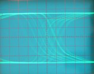
I attached some oscillograms illustrating Toslink jitter
Oscillogram #1, XTOS SPDIF output, 192 KHz
Oscillogram #2, Optical receiver output, 1 meter plastic fiber, 192 KHz
Oscillogram #3, Optical receiver output, 5 meter plastic fiber, 192 KHz.
Oscillogram #4, optical receiver output , 5 meter plastic fiber, 44.1 KHz.
Measured jitter increases with increasing sample rate and fiber interlink length. When applying pressure on the fiber interlink (stand on it) data corruption occurs due to temporary deformation of the fiber. So it is advised to keep the fiber free of mechanical stress (pulling, bending).
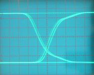
High jitter is measured at the Toslink optical receiver, regardless of Toslink source jitter. However, the recovered PLL clock from a good quality receiver like WM8804, DIR9001, DIX9211 does not show any significant increase in jitter. PLL recovered clock jitter remains around specified 50ps regardless of input jitter.
Oscillogram #5, PLL recovered clock
But 50ps is still too high …..
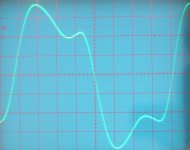
The passive clock further attenuates jitter that is still present in the PLL recovered clock by up to 174 dB.
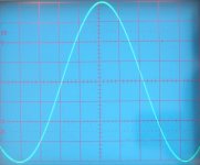
Oscillogram #6 shows the 24.576 MHz passive clock output.
It is a sine wave with extremely high spectral purity. Even the best masterclocks would have big problems generating something that even comes close to this almost perfect sine wave. The passive clock tracks the input clock so it always runs in perfect sync with the source clock.
Because the passive clock does not require a power supply and does not contain any semiconductors it can always offer lower phase noise and lower deterministic jitter than any other conventional crystal oscillator. This is about as good as it gets.
-> Toslink jitter issue solved.
Jitter and interference also enter through I2S signals, so all data and I2S signals throughout the Mosaic T DAC are synchronously reclocked by a synchronous reclocker array in order to maintain extremely low jitter and noise throughout the DAC circuits. The limited 13 MHz interface bandwidth (Toslink, 192 KHz) reduces unwanted spreading over the DAC circuits and keeps the DAC output signal clean regardless of source interference.
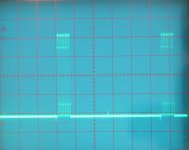
The Multi-stream decoder also attenuates I2S interference by 87.5% because it runs in data burst mode with 12.5% data density. This reduces average I2S interference by 87.5% as following oscillogram shows.
Oscillogram #7, multi-stream interface data burst clock signal that is used to pump multi-stream serial data into the Mosaic DAC core. The burst clock frequency equals 12.288 MHz here (192 Khz sample rate). The small glitch between the clock busts is caused by the latching signal TLE that is used for output sample timing.
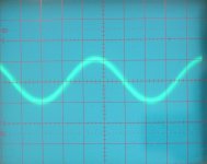
The final oscillogram #8 shows a -60dB sine wave (completely unfiltered output signal!) generated by the Mosaic T DAC. I used a 5 meter plastic Toslink fiber and 192 KHz sample rate in order to create worst case conditions illustrated by previous oscillograms.
I use a noisy PC and a XTOS USB to Toslink converter.
Scope is on max. sensitivity (2mV/div) and the prope is set 1:1. When short circuiting the scope probe with this sensitivity setting I get similar amount of noise. So the visible noise on the -60dB signal is mainly the result of the oscilloscope noise floor.
As you can see there are no glitches, even at 192 KHz sample rate, and DLE error is vanishing low. This is one of the advantages of the novel common-rail matrix concept. This oscillogram also shows how clean the unfiltered output signal gets when HF source interference is effectively blocked and ground loops are completely eliminated.
Passive clock??
I recall you mentioning that your master clock somehow makes use of fuzzy logic technology. Can you elaborate a bit?
The fuzzy logic clock is only used in the Mosaic USB DAC. The USB DAC is master and it runs on a discrete local crystal oscillator. The clock is distributed as follows:
Masterclock -> XMOS audio clock -> I2S -> DAC (data).
Masterclock -> programmable divider -> Latch signal -> DAC (sample timing).
I2S and sample timing clocks are separated in order to obtain cleanest sample timing clock.
The divided down Latch signal may cause data corruption as the counter can start at op to 128 random positions in relation to the I2S signal. The fuzzy logic circuit detects when the Latch signal coincides with the I2S signal and resets the counter once after such event. Then the Latch signal will be lined up correctly.
The divider is programmable in order to generate 44.1/48, 88.2/96, and 176.4/192 KHz. Division factor is selected as follows:
XMOS sample rate detection -> sample rate indicator LEDs -> decoder / multiplexer.
Problems with this configuration:
The DAC only works with USB audio sources, cannot connect audiophile CD-players & CD transports for example.
I2S signals still feed large bandwidth (GHz) interference into the Mosaic DAC. When synchronous reclockers are used to clean up these I2S signals the masterclock gets polluted as this GHz bandwidth interference spectrum very easily spreads over small stray capacitances in the pF range.
Crystal oscillators (masterclocks) are -extremely- sensitive to power supply noise and semiconductor noise (FETs / transistors used in the crystal oscillator. Even cleanest battery power supplies and low noise semiconductors still produce too much phase noise and result in a unique phase noise spectrum and related sound.
Because the phase noise spectrum keeps changing (ambient temperature, oscillator drift, interference spectrum) the sound quality keeps changing too.
The solution:
The XMOS USB receiver is moved outside the DAC enclosure, preferably a few meters away so the DAC won’t pick up any interference from the XMOS.
Toslink is used to completely eliminate ground loops and limit source / XMOS interference bandwidth to only 13 MHz. Chip isolators don’t work as GHz bandwidth source interference easily passes chip isolator stray capacitance.
The next problem, Toslink jitter:
I attached some oscillograms illustrating Toslink jitter
Oscillogram #1, XTOS SPDIF output, 192 KHz
Oscillogram #2, Optical receiver output, 1 meter plastic fiber, 192 KHz
Oscillogram #3, Optical receiver output, 5 meter plastic fiber, 192 KHz.
Oscillogram #4, optical receiver output , 5 meter plastic fiber, 44.1 KHz.
Measured jitter increases with increasing sample rate and fiber interlink length. When applying pressure on the fiber interlink (stand on it) data corruption occurs due to temporary deformation of the fiber. So it is advised to keep the fiber free of mechanical stress (pulling, bending).
High jitter is measured at the Toslink optical receiver, regardless of Toslink source jitter. However, the recovered PLL clock from a good quality receiver like WM8804, DIR9001, DIX9211 does not show any significant increase in jitter. PLL recovered clock jitter remains around specified 50ps regardless of input jitter.
Oscillogram #5, PLL recovered clock
But 50ps is still too high …..
The passive clock further attenuates jitter that is still present in the PLL recovered clock by up to 174 dB.
Oscillogram #6 shows the 24.576 MHz passive clock output.
It is a sine wave with extremely high spectral purity. Even the best masterclocks would have big problems generating something that even comes close to this almost perfect sine wave. The passive clock tracks the input clock so it always runs in perfect sync with the source clock.
Because the passive clock does not require a power supply and does not contain any semiconductors it can always offer lower phase noise and lower deterministic jitter than any other conventional crystal oscillator. This is about as good as it gets.
-> Toslink jitter issue solved.
Jitter and interference also enter through I2S signals, so all data and I2S signals throughout the Mosaic T DAC are synchronously reclocked by a synchronous reclocker array in order to maintain extremely low jitter and noise throughout the DAC circuits. The limited 13 MHz interface bandwidth (Toslink, 192 KHz) reduces unwanted spreading over the DAC circuits and keeps the DAC output signal clean regardless of source interference.
The Multi-stream decoder also attenuates I2S interference by 87.5% because it runs in data burst mode with 12.5% data density. This reduces average I2S interference by 87.5% as following oscillogram shows.
Oscillogram #7, multi-stream interface data burst clock signal that is used to pump multi-stream serial data into the Mosaic DAC core. The burst clock frequency equals 12.288 MHz here (192 Khz sample rate). The small glitch between the clock busts is caused by the latching signal TLE that is used for output sample timing.
The final oscillogram #8 shows a -60dB sine wave (completely unfiltered output signal!) generated by the Mosaic T DAC. I used a 5 meter plastic Toslink fiber and 192 KHz sample rate in order to create worst case conditions illustrated by previous oscillograms.
I use a noisy PC and a XTOS USB to Toslink converter.
Scope is on max. sensitivity (2mV/div) and the prope is set 1:1. When short circuiting the scope probe with this sensitivity setting I get similar amount of noise. So the visible noise on the -60dB signal is mainly the result of the oscilloscope noise floor.
As you can see there are no glitches, even at 192 KHz sample rate, and DLE error is vanishing low. This is one of the advantages of the novel common-rail matrix concept. This oscillogram also shows how clean the unfiltered output signal gets when HF source interference is effectively blocked and ground loops are completely eliminated.
Attachments
-
 XTOS-192K-SPDIF.jpg95 KB · Views: 919
 -
 optical-192K-1m.jpg96.2 KB · Views: 897
 -
 optical-192K-5m.jpg88.9 KB · Views: 886
 -
 optical-44K1-5m.jpg93.8 KB · Views: 810
 -
 PLL-recovered-clock.jpg93.5 KB · Views: 812
 -
 24M-passive-clock-out.jpg98.4 KB · Views: 149
 -
 12M- Mosaic-clock burst.jpg81.3 KB · Views: 145
 -
 Mosaic-1K-60dB-192K.jpg90.6 KB · Views: 148
Last edited:
Hi John,
when playing music from a computer and having a preamp as receiving end, would you recommend using USB out with your XTOS into the Mosaic T, or rather using a soundcard that directly outputs Toslink into the Mosaic T? Which setup will be 'better' in terms of jitter, HF modulations etc. and thus in measurable results?
Thank you,
Robert
...The passive clock further attenuates jitter that is still present in the PLL recovered clock by up to 174 dB.
Oscillogram #6 shows the 24.576 MHz passive clock output.
It is a sine wave with extremely high spectral purity. Even the best masterclocks would have big problems generating something that even comes close to this almost perfect sine wave. The passive clock tracks the input clock so it always runs in perfect sync with the source clock.
Because the passive clock does not require a power supply and does not contain any semiconductors it can always offer lower phase noise and lower deterministic jitter than any other conventional crystal oscillator. This is about as good as it gets...
John, thank you, for such an comprehensive response.
Regarding your particularly intriguing passive clocking, from your above description it seems that it may be some form of very high-Q filter, possibly a multi-element crystal lattice bandpass filter, as were once common in RF applications. However, that you also describe your passive clock as being able to track the recovered input source clock frequency argues against my guess of a passive high-Q bandpass filter - at least, not without an electronically tunable center frequency via some active element.
Were you able to measure the close in phase noise rejection of the passive circuit, say at a 10Hz to 1Hz carrier offset?
If you prefer, please feel free to respond via PM.
Thanks.
Last edited:
Jitter and interference also enter through I2S signals, so all data and I2S signals throughout the Mosaic T DAC are synchronously reclocked by a synchronous reclocker array in order to maintain extremely low jitter and noise throughout the DAC circuits.
Wouldn't it be nice that the Mosaic had an I2S input connection?
We could for example connect a dedicated, battery powered, optimised SD player, with very short interconnect, for added versatility.
Cheers,
M.
 Now I have to make this on every site I can.
No, no
M.
it"s your fault you decide to live so far away

i'v got one on order and the shipping cost is luckily very reasonable
- Home
- Source & Line
- Digital Line Level
- Building the ultimate NOS DAC using TDA1541A