Hi, -ecdesigns-TDA1541A datasheet page 4...
Right, however:
"When input OB/TWC input is connected to VDD1 the two channels of data (L/R) are input simultaneously via DATA L and DATAR, accompanied with BCK and a latch-enable input (LE). With this mode selected the data must be in offset binary. The converted samples appear at the output at the positive going transition of the latch enable signal."
That is to say signal LE also important, at least once, at mode of the simultaneous data loading.
Apropos, recommend to read if there is possibility van de Plassche monograph. He is one of the developer TDA1540/1541(A) family.
That will say about garbling the square-wave pulse (the post # 4530)? Possible, HF decline, about which spoke guido in post #32, is connected with reduction SR?
Since begin given subject passed 6 years. Some your beliefs could change. Could you lead certain summation, like post #73? On what decisions stopped you on given moment?
Serg
hi ecdesigns, so humbled that you replied to my post ")
i currently have the receiver chips bypassed to a te7022- 1541 via i2s. after one listen i figured that all the bad rep 1541 gets is due to the 7220.
the hiss was solved by swapping out some caps in the ps. no doubt it's a poorly designed one...
could you please outline for me the reason for different output transistor choices from mark3 and upwards?
thanks
I just did a bit of googling, and this is the thread I meant, look at post #35 and #123, it's a full recipe of a tda1541a dac.
http://www.diyaudio.com/forums/digital-line-level/203511-any-good-tda1541a-dac-kit-4.html
Actually, be sure to read the WHOLE thread, not just the recipe! It talks about grounding, decoupling, layout, power supplies, I2S conditioning, DEM reclocking, the whole bloody thing. It's a gold mine!
http://www.diyaudio.com/forums/digital-line-level/203511-any-good-tda1541a-dac-kit-4.html
Actually, be sure to read the WHOLE thread, not just the recipe! It talks about grounding, decoupling, layout, power supplies, I2S conditioning, DEM reclocking, the whole bloody thing. It's a gold mine!
I just did a bit of googling, and this is the thread I meant, look at post #35 and #123, it's a full recipe of a tda1541a dac.
http://www.diyaudio.com/forums/digital-line-level/203511-any-good-tda1541a-dac-kit-4.html
Actually, be sure to read the WHOLE thread, not just the recipe! It talks about grounding, decoupling, layout, power supplies, I2S conditioning, DEM reclocking, the whole bloody thing. It's a gold mine!
ahaa, yes, have that good thread as well, reminder for my local audio friend
Hi SSerg,
I use time multiplex mode and two's complement (/OB/TWC connected to 5V) exclusively.
1) Direct interpolation was abandoned mainly because of trebles roll-off.
2) External DAC concept was abandoned because I wasn't able to fully block source jitter.
3) SD-transport concept was developed to approximate an ideal digital audio source.
The main reason I kept changing the design, designing and building one version after the other was increasing / changing mains interference spectrum that resulted in varying DAC performance levels. I wasn't aware of this at first, and this has lead to wrong conclusions.
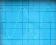
I attached an oscillogram showing my mains voltage when interference levels are lowest. Most irritating interference is the approx. 2.5 KHz signal riding on the mains. This interference swithes "on" and "off" with random intervals.
The interference is generated outside my house as it persists when my house installation is completely disconnected from the mains.
Ken Newton reported similar mains distortion, perhaps this mains interference is a global thing.
I would be very interested if people from other countries have similar distortion on the mains. If you have a scope the interference can be measured safely by connecting the scope probe tip to a sheet of copper. This will pick up 50 or 60 Hz mains frequency and the interference riding on it (when present). Measure for longer time period like a quarter of an hour because this interference switches on/off periodically.
Knowing the cause of the problem I redesigned power supplies so they are immune to this interference.
Similar, I had to design yet another masterclock that is immune to (power supply) interference. It will always produce ultra low jitter, regardless of external conditions and clock loading.
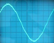
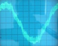
Next oscillogram shows the 11.2896 Mhz output signal. It's a pure sine wave with very low distortion (fundamental).
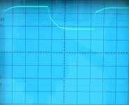
The third oscillogram shows the BCK attenuator output signal. The signal is band limited in order to minimise ground-bounce. The positive transient that's very important for sample timing is speeded up to maximum in order to ensure maximum trigger certainty.
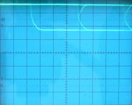
The final oscillogram shows the band limited and attenuated DATA signal. This signal is derived straight from the DSP on the SD8-transport.
That is to say signal LE also important, at least once, at mode of the simultaneous data loading.
I use time multiplex mode and two's complement (/OB/TWC connected to 5V) exclusively.
Since begin given subject passed 6 years. Some your beliefs could change. Could you lead certain summation, like post #73? On what decisions stopped you on given moment?
1) Direct interpolation was abandoned mainly because of trebles roll-off.
2) External DAC concept was abandoned because I wasn't able to fully block source jitter.
3) SD-transport concept was developed to approximate an ideal digital audio source.
The main reason I kept changing the design, designing and building one version after the other was increasing / changing mains interference spectrum that resulted in varying DAC performance levels. I wasn't aware of this at first, and this has lead to wrong conclusions.
I attached an oscillogram showing my mains voltage when interference levels are lowest. Most irritating interference is the approx. 2.5 KHz signal riding on the mains. This interference swithes "on" and "off" with random intervals.
The interference is generated outside my house as it persists when my house installation is completely disconnected from the mains.
Ken Newton reported similar mains distortion, perhaps this mains interference is a global thing.
I would be very interested if people from other countries have similar distortion on the mains. If you have a scope the interference can be measured safely by connecting the scope probe tip to a sheet of copper. This will pick up 50 or 60 Hz mains frequency and the interference riding on it (when present). Measure for longer time period like a quarter of an hour because this interference switches on/off periodically.
Knowing the cause of the problem I redesigned power supplies so they are immune to this interference.
Similar, I had to design yet another masterclock that is immune to (power supply) interference. It will always produce ultra low jitter, regardless of external conditions and clock loading.
Next oscillogram shows the 11.2896 Mhz output signal. It's a pure sine wave with very low distortion (fundamental).
The third oscillogram shows the BCK attenuator output signal. The signal is band limited in order to minimise ground-bounce. The positive transient that's very important for sample timing is speeded up to maximum in order to ensure maximum trigger certainty.
The final oscillogram shows the band limited and attenuated DATA signal. This signal is derived straight from the DSP on the SD8-transport.
Attachments
…
The main reason I kept changing the design, designing and building one version after the other was increasing / changing mains interference spectrum that resulted in varying DAC performance levels. I wasn't aware of this at first, and this has lead to wrong conclusions.
…
The interference is generated outside my house as it persists when my house installation is completely disconnected from the mains.
…
I would be very interested if people from other countries have similar distortion on the mains.
Hi John,
Mains interferences are well known phenomena, very old news.
On my stereo/home theater setup there are 4 isolation transformers, the secondary windings are balanced to the ground, with capacitors filters after the secondary windings. Their positive impact on the sound quality of my setup is big.
Some (if not most) of the interference on the mains is on RF. As we know, RF spreads also by radiation, not only by conduction. Ideally, RF interference should be killed, or minimized, before they enter any audio gear.
On the part of designing and building audio gear, RF interference should be killed, or minimized, right at the mains voltage entrance to the equipment, with a good shield completely surrounding the mains filter. In addition to that, the power supply should be very well filtered, since there is no practical mains filter that kills completely all RF interference present on the mains supply.
Extra care should be taken when designing mains filter, to ensure that such a filter is capable of withstanding consumption variations by the equipment, without fluctuations to its' output voltage.
In addition, the equipment housing, or case, should have a very good and efficient RF shielding, since there are RF waves in all (or most) house rooms. Those RF waves come from radio, TV and communication equipment outside the house, as well as from sources inside the house, like cellular phones, cordless phones, computers, refrigerators motors, TV sets, all equipment that have switching power supplies and all equipment having digital circuits. Most of the commercial equipment do not have adequate shielding (it's too expansive).
Hi John,
Mains interferences are well known phenomena, very old news.
So, then, what is the explanation for why John and I both see significant 2.5kHz noise bursts riding the mains supply, despite power conditioning and ground loop elimination?
So, if the noise is not system-related, and not mains-induced, then it is RF pickup.
There are some ways of dealing with it - you call your's circuit as "RF receiver", and try to make it worse.
That long speaker wires connect to mains ground - look, you can easily make a simple radio with that!
There are some ways of dealing with it - you call your's circuit as "RF receiver", and try to make it worse.
That long speaker wires connect to mains ground - look, you can easily make a simple radio with that!
At first I was thinking it might be PLC injected by the utility for control signals, but that is typically at 24k and up. Wifi is 2.4ghz. 2.5k is a very low frequency for communications. Hard to imagine what is putting out such a low frequency. Is it just from motors powered by the same feed as your house? Don't most motors run at 2400 rpm? ie 2.4k? Perhaps it is nothing more than the refrigerator or furnace fans on the same transformer on the street.
So, then, what is the explanation for why John and I both see significant 2.5kHz noise bursts riding the mains supply, despite power conditioning and ground loop elimination?
I have no idea about those 2.5KHz noise bursts.
I do know that there is RF on the mains supply.
I do know, by experience, that isolation transformers on the mains supply have a significant positive impact on the sound quality of my setup.
I do know that there are RF waves in my living room (I receive FM transmissions, my cordless phone and my cellular phone work there).
I do know that RF waves propagate by radiation, as well as by conduction.
Hi s3tup
Simultaneous mode on the TDA1541A is intended for 8 times oversampling (bit clock frequency limitations). I do not need this. It is also more difficult to extract an ultra low jitter 44.1 KHz latch signal from a 11.2896 MHz masterclock.
The MCU uses on-chip hardware to generate I2S, this hardware does not support simultaneous mode. Toggling I/O pins by software would require far more powerful MCU's and these would generate far more interference / jitter levels on the I/O pins. The MCU in the SD8-transport runs on lowest possible clock frequency (56.488 MHz) and highly efficient code (software) to keep interference levels on I2S, power supply and GND as low as possible. Side effect is very low power consumption during playback of approx. 100 milliwatts.
I measure jitter by using a tunable, narrow bandwidth bandpass filter. Jitter is now translated into amplitude modulation (amplitude of signal drops when its frequency is slightly higher or lower than that of the tuned bandpass filter). This signal can then be demodulated and amplified very similar as with an AM radio receiver.
The signal can then be fed to a spectrum analyser. But the resulting spectrum tells very little if anything about its effects on perceived sound.
However, the key issue with jitter seems to be jitter spectrum. So the main problem would be interpreting the effects of jitter spectrum on complex signals like music. After all the final goal of all these tests and measurements is approaching the perceived sound quality of true analogue audio souces like studio tape or Vinyl.
Therefore I think it is necessary to perform listening tests with very familiar high quality reference recordings (Closer to the music vol. 1 … 4 from Stockfish records for example). This in order to make sure that the jitter spectrum no longer leads to audible distortion.
Some important things to listen for are focus, background noise, clarity of vocals and purity of tones (piano).
The 2.5 KHz is modulated on the mains outside my house. I can filter it out using a mains lowpass filter with approx. 500Hz ! turnover frequency. The interference passes conventional mains filters because these are designed to filter out radio frequencies and thus have much higher turnover frequency.
Since the signal rides on all mains wiring in the house it also produces electrical fields that can be picked up wirelessly by equipment and interlinks.
So the mains filters must be placed as close to the mains entry point as possible in order to keep the 2.5 KHz interference away from mains wiring and preventing it from spreading all over the house.
2.5 Khz can be filtered out by a 500Hz low pass filter if you know it's present on the mains. The problem however was that I didn't expect such very strong low frequency interference on the mains and I didn't expect it to appear and completely disappear at random intervals (varies between seconds and days).
Measurements carried out together with a technician of my energy supplier showed that the interference is generated outside my house (so it is not caused by any equipment I use in my house). The interference also passes a distribution transformer up the road because the frequency is so low. This interference seems to be well within specifications and the energy supplier will take no further action.
If you already use yours MCU and have a grip on the data/clock traces, why won't you use TDA in simultaneous load mode?
Simultaneous mode on the TDA1541A is intended for 8 times oversampling (bit clock frequency limitations). I do not need this. It is also more difficult to extract an ultra low jitter 44.1 KHz latch signal from a 11.2896 MHz masterclock.
The MCU uses on-chip hardware to generate I2S, this hardware does not support simultaneous mode. Toggling I/O pins by software would require far more powerful MCU's and these would generate far more interference / jitter levels on the I/O pins. The MCU in the SD8-transport runs on lowest possible clock frequency (56.488 MHz) and highly efficient code (software) to keep interference levels on I2S, power supply and GND as low as possible. Side effect is very low power consumption during playback of approx. 100 milliwatts.
How do you know your's clock is low jitter, i mean have you measured it with an equipment which has less jitter than your clock?
I measure jitter by using a tunable, narrow bandwidth bandpass filter. Jitter is now translated into amplitude modulation (amplitude of signal drops when its frequency is slightly higher or lower than that of the tuned bandpass filter). This signal can then be demodulated and amplified very similar as with an AM radio receiver.
The signal can then be fed to a spectrum analyser. But the resulting spectrum tells very little if anything about its effects on perceived sound.
However, the key issue with jitter seems to be jitter spectrum. So the main problem would be interpreting the effects of jitter spectrum on complex signals like music. After all the final goal of all these tests and measurements is approaching the perceived sound quality of true analogue audio souces like studio tape or Vinyl.
Therefore I think it is necessary to perform listening tests with very familiar high quality reference recordings (Closer to the music vol. 1 … 4 from Stockfish records for example). This in order to make sure that the jitter spectrum no longer leads to audible distortion.
Some important things to listen for are focus, background noise, clarity of vocals and purity of tones (piano).
So, if the noise is not system-related, and not mains-induced, then it is RF pickup.
The 2.5 KHz is modulated on the mains outside my house. I can filter it out using a mains lowpass filter with approx. 500Hz ! turnover frequency. The interference passes conventional mains filters because these are designed to filter out radio frequencies and thus have much higher turnover frequency.
Since the signal rides on all mains wiring in the house it also produces electrical fields that can be picked up wirelessly by equipment and interlinks.
So the mains filters must be placed as close to the mains entry point as possible in order to keep the 2.5 KHz interference away from mains wiring and preventing it from spreading all over the house.
There are some ways of dealing with it - you call your's circuit as "RF receiver", and try to make it worse.
2.5 Khz can be filtered out by a 500Hz low pass filter if you know it's present on the mains. The problem however was that I didn't expect such very strong low frequency interference on the mains and I didn't expect it to appear and completely disappear at random intervals (varies between seconds and days).
Measurements carried out together with a technician of my energy supplier showed that the interference is generated outside my house (so it is not caused by any equipment I use in my house). The interference also passes a distribution transformer up the road because the frequency is so low. This interference seems to be well within specifications and the energy supplier will take no further action.
Here some mains interference pictures just captured today.
First picture shows 2.5 KHz interference when it is starting to peak (it gets even higher!)
Second picture just captured seconds later, the 2.5 KHz interference has gone for a moment.
I also have periodic mains drop-outs (few milliseconds to seconds) as cars pass by (loose connection in distribution point / arcing).
Attachments

ecdesigns,
Earlier in this thread you experimented with battery power. You have not revisited this avenue, so can one assume that despite the mains polution you speak of presently, battery power is still inferior in your opinion...or is it just less practical in terms of usage?
Earlier in this thread you experimented with battery power. You have not revisited this avenue, so can one assume that despite the mains polution you speak of presently, battery power is still inferior in your opinion...or is it just less practical in terms of usage?
Hi all, I am planning to run the I2S out from CS8412 to a PCM63 dac. Has this forum decided on the best way to glue the I2S output to a 2's complement DAC? I've seen 74HC176 used as a shift register, but have seen alternative arrangements as well.
Some q:
1. Can data be sent straight through from cs8412 to PCm63?
2. If so, would you then invert BCK with a 74HC04 while passing LE/WordCK through 2x HC176?
Thanks guys!
Some q:
1. Can data be sent straight through from cs8412 to PCm63?
2. If so, would you then invert BCK with a 74HC04 while passing LE/WordCK through 2x HC176?
Thanks guys!
- Home
- Source & Line
- Digital Line Level
- Building the ultimate NOS DAC using TDA1541A