Hi Dr.H,
Driver, TTL to differential, connect to masterclock:
TEXAS INSTRUMENTS|SN65LVDS1DBVT|LVDS DRIVER, SMD, 65LVDS1, SOT | Farnell Nederland
Receiver, differential to TTL, connect to digital audio source:
TEXAS INSTRUMENTS|SN65LVDS2DBVR|IC, LINE RECEIVER, 5-SOT23 | Farnell Nederland
Line termination 110 Ohm.
You need an ultra fast divider using separate D flip-flops with separate power supply decoupling.
Discrete Johnson counter can be constructed using following flip-flops (3 D flip-flops required):
TEXAS INSTRUMENTS|SN74AUC1G74DCUR|LOGIC, 74AUC1G, D FLIP FLOP, US8 | Farnell Nederland
FAIRCHILD SEMICONDUCTOR|NC7SV74K8X|IC, SM, LOGIC, NC7SV, FLIP-FLOP | Farnell Nederland
Connect all 3 clock inputs to the masterclock.
Q output of flip-flop 1 connects to D input of flip-flop2
Q output of flip-flop 2 connects to D input of flip-flop3
/Q output of flip-flop 3 connects to D input of flip-flop1
preset & clear inputs of all flip-flops connect to plus.
divide-by-8 clock signal is present on Q and /Q outputs of all 3 flip-flops.
If it is not possible to synchronize both DAC and source you can invert the clock signal by swapping transceivers differential inputs
Yes, the transport servo may lock-out (depending on design). This could result in very high disc speed. So always remove disc before powering up.
You could add a small relay that powers-up / connects a second backup masterclock in the transport when no external clock is detected. Clock detector can be constructed using a one-shot circuit:
The One-shot Monostable Multivibrator
Pulse duration must be (much) longer than pulse duration of the masterclock signal.
The output of the one shot circuit can drive a small relay using a transistor for example.
Construct the circuit such way that the backup masterclock is powered up / connected when there is no power on the relay using NC relay contacts. Use one contact to apply power to the back-up clock and the other to toggle between backup and external clock signal. Connect backup clock to relay NC (normally closed) contact and external clock to NO (normally open) contact.
1. What buffer would you suggest for the clock?
Driver, TTL to differential, connect to masterclock:
TEXAS INSTRUMENTS|SN65LVDS1DBVT|LVDS DRIVER, SMD, 65LVDS1, SOT | Farnell Nederland
Receiver, differential to TTL, connect to digital audio source:
TEXAS INSTRUMENTS|SN65LVDS2DBVR|IC, LINE RECEIVER, 5-SOT23 | Farnell Nederland
Line termination 110 Ohm.
2. What divider would you suggest?
You need an ultra fast divider using separate D flip-flops with separate power supply decoupling.
Discrete Johnson counter can be constructed using following flip-flops (3 D flip-flops required):
TEXAS INSTRUMENTS|SN74AUC1G74DCUR|LOGIC, 74AUC1G, D FLIP FLOP, US8 | Farnell Nederland
FAIRCHILD SEMICONDUCTOR|NC7SV74K8X|IC, SM, LOGIC, NC7SV, FLIP-FLOP | Farnell Nederland
Connect all 3 clock inputs to the masterclock.
Q output of flip-flop 1 connects to D input of flip-flop2
Q output of flip-flop 2 connects to D input of flip-flop3
/Q output of flip-flop 3 connects to D input of flip-flop1
preset & clear inputs of all flip-flops connect to plus.
divide-by-8 clock signal is present on Q and /Q outputs of all 3 flip-flops.
And also, would I need to invert the clock that is sent back to the transport?
If it is not possible to synchronize both DAC and source you can invert the clock signal by swapping transceivers differential inputs
Finally, if the transport starts up without a clock (say the dac is off) is there a risk the transport latches up?
Yes, the transport servo may lock-out (depending on design). This could result in very high disc speed. So always remove disc before powering up.
You could add a small relay that powers-up / connects a second backup masterclock in the transport when no external clock is detected. Clock detector can be constructed using a one-shot circuit:
The One-shot Monostable Multivibrator
Pulse duration must be (much) longer than pulse duration of the masterclock signal.
The output of the one shot circuit can drive a small relay using a transistor for example.
Construct the circuit such way that the backup masterclock is powered up / connected when there is no power on the relay using NC relay contacts. Use one contact to apply power to the back-up clock and the other to toggle between backup and external clock signal. Connect backup clock to relay NC (normally closed) contact and external clock to NO (normally open) contact.
Hi Dr.H,
The TDA1543 is powered by the +5V TDA1541A supply. This consists of a balanced capacitance multiplier followed by a balanced filtered-buffered zener regulator.
spectrum.
Hi John,
can You explain the difference between balanced supply and the previously used
common mode supply. Can You please post a schematic of the balanced capacitance multiplier followed by a balanced filtered-buffered zener regulator.
Hi JOSI1,
Common mode circuits, first capacitance multiplier / regulator references to the smoothing cap, second capacitance multiplier / regulator references to first one.
Balanced mode circuits, first capacitance multiplier / regulator references to second one. Second capacitance multiplier/ regulator references to first one.
Latest measurements (using low value capacitors to increase ripple voltage by factor 5,000) showed that the common mode version offers lowest ripple voltage levels. So This is the version I am planning to use.
I also plan to combine capacitance multiplier and regulator sections in one circuit. I need two of these in cascade to get low enough ripple voltage levels.
The schematics of these combined circuits aren't final yet.
can You explain the difference between balanced supply and the previously used
common mode supply. Can You please post a schematic of the balanced capacitance multiplier followed by a balanced filtered-buffered zener regulator.
Common mode circuits, first capacitance multiplier / regulator references to the smoothing cap, second capacitance multiplier / regulator references to first one.
Balanced mode circuits, first capacitance multiplier / regulator references to second one. Second capacitance multiplier/ regulator references to first one.
Latest measurements (using low value capacitors to increase ripple voltage by factor 5,000) showed that the common mode version offers lowest ripple voltage levels. So This is the version I am planning to use.
I also plan to combine capacitance multiplier and regulator sections in one circuit. I need two of these in cascade to get low enough ripple voltage levels.
The schematics of these combined circuits aren't final yet.
Mk7 & Mk8 Clocks/Reshnchronization Circuits
Hi EC Designs / John,
Thank you for your enormous effort and generous attitude about sharing your work, as I (like so many others) appreciate what you have done.")
Regarding the digital/clock/reclocking circuits on the Mk7 & Mk8, which one of these do you plan to use in your next planned board?
It's not really clear what advantage - other than simplicity - in the clocking and synchronization circuits between the Mk8 & Mk7 that you discovered.
Any possibility that with the power supply changes at the same time as the clock changes in the Mk7 to Mk8 there may have been a cumulative (possibly negating) impact, if indeed the clock had some contribution?
Regards,
Gary
Hi EC Designs / John,
Thank you for your enormous effort and generous attitude about sharing your work, as I (like so many others) appreciate what you have done.
Regarding the digital/clock/reclocking circuits on the Mk7 & Mk8, which one of these do you plan to use in your next planned board?
It's not really clear what advantage - other than simplicity - in the clocking and synchronization circuits between the Mk8 & Mk7 that you discovered.
Any possibility that with the power supply changes at the same time as the clock changes in the Mk7 to Mk8 there may have been a cumulative (possibly negating) impact, if indeed the clock had some contribution?
Regards,
Gary
Hi roger57,
None of them. I now use a sub-miniature timing module that generates 11.2896 MHz clock (3Vpp) for SD-transport and 2.8224 MHz (1.8Vpp) clock for TDA1541A and DEM soft-sync. Module measures 12mm x 32mm x 6mm.
DATA and WS are no longer reclocked, more problems than advantages (interference).
I2S attenuators could be removed as all generated I2S signals now have 1.8Vpp signal amplitude (level translators on DATA / WS and 1.8Vpp BCK signal from the timing module).
Yes this could be possible, but MK7 and MK8 power supply and clock circuits are no longer used in the latest MK9 prototype setup.
Regarding the digital/clock/reclocking circuits on the Mk7 & Mk8, which one of these do you plan to use in your next planned board?
None of them. I now use a sub-miniature timing module that generates 11.2896 MHz clock (3Vpp) for SD-transport and 2.8224 MHz (1.8Vpp) clock for TDA1541A and DEM soft-sync. Module measures 12mm x 32mm x 6mm.
DATA and WS are no longer reclocked, more problems than advantages (interference).
I2S attenuators could be removed as all generated I2S signals now have 1.8Vpp signal amplitude (level translators on DATA / WS and 1.8Vpp BCK signal from the timing module).
Any possibility that with the power supply changes at the same time as the clock changes in the Mk7 to Mk8 there may have been a cumulative (possibly negating) impact, if indeed the clock had some contribution?
Yes this could be possible, but MK7 and MK8 power supply and clock circuits are no longer used in the latest MK9 prototype setup.
I2S attenuators could be removed as all generated I2S signals now have 1.8Vpp signal amplitude (level translators on DATA / WS and 1.8Vpp BCK signal from the timing module).
Maybe you are using this: SY100EPT22VKI ?
Kind regards,
To Clock...or to reclock (not!)
John,
The DEM circuits are still part of the function of the clock board? I imagine you are not changing how these are generated and connected?
Regards,
Gary
Hi roger57,
DATA and WS are no longer reclocked, more problems than advantages (interference).
John,
The DEM circuits are still part of the function of the clock board? I imagine you are not changing how these are generated and connected?
Regards,
Gary
Hi galeb,
No, (P)ECL gives too low output voltage swing to drive the TDA1541A. I use UHS buffers running on 1.8V power supply with series resistors on the inputs:
FAIRCHILD SEMICONDUCTOR|NC7NZ34K8X|IC, NC7NZ TINY, SMD, US-8 | Farnell Nederland
BCK synchronous divide-by-4 circuit runs on 1.8V power supply so it outputs 1.8Vpp.
Maybe you are using this: SY100EPT22VKI ?
No, (P)ECL gives too low output voltage swing to drive the TDA1541A. I use UHS buffers running on 1.8V power supply with series resistors on the inputs:
FAIRCHILD SEMICONDUCTOR|NC7NZ34K8X|IC, NC7NZ TINY, SMD, US-8 | Farnell Nederland
BCK synchronous divide-by-4 circuit runs on 1.8V power supply so it outputs 1.8Vpp.
Hi roger57,
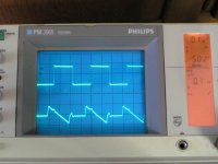
TDA1541A DEM oscillator is now soft-synced with 2.8224 MHz bit clock (attached picture). Sync signal is now taken from pin 2 (BCK) only.
Upper trace shows bit clock (amplitude equals approx. 1.9Vpp). Lower trace shows DEM clock signal (amplitude equals approx. 900mVpp). The spikes on the DEM clock sawtooth signal are caused by synchronization by BCK.
The bit clock is derived from the masterclock using two UHS D flip-flops that form a synchronous divide-by-4 Johnson counter.
Both, new masterclock module and better performing DEM clock resulted in more transparency and more unmasked flaws.
Now the voltage regulators (that performed similar to battery power supply) turned out to be the bottleneck. I needed much more quiet supplies with better load regulation / lower impedance over much larger bandwidth.
After many measurements and listening tests, a 2-stage common mode ripple rejector feeding a precision shunt regulator through a balanced resistor current limiter performed best. These common-mode shunt regulators are now used for SD-transport (3V3), masterclock (3V6), and TDA1541A (5V, -5V, -15V).
The shunt regulators are based on high-gain Darlingtons (ft = 160 MHz, HFe = 3000), a temperature compensated NPN transistor and a filtered LED reference. Low noise bandgap references (bipolar & FET) and zener diodes produced much higher noise levels that couldn't be filtered out properly.
The DAC output stage is now based on SMD RF JFETs that are used as current buffer. The JFETs require adjustable negative gate voltage (0 ... -5V).
The new voltage regulators and current buffers further increased transparency, now revealing resistor noise spectrum issues. Some critical resistors in volume control and Circlotron power amp had to be changed to hybrid resistors in order to fine-tune the system noise spectrum. The hybrid resistors consist of the right "mix" of bulk metal foil, carbon composition, metal film and wire-wound resistors.
So I am currently concentrating on the last bits like system noise floor frequency spectrum.
The resistor tuning revealed some flaws with SD-transport noise spectrum. The SD-transport is already one of the cleanest digital audio sources around (very low interference on power supplies and I2S outputs and very low jitter on DATA & WS). The bit clock (determines sample timing with the TDA1541A) is taken from the masterclock. The bit clock from the SD-transport is not used.
My brother is now writing software for a new single-chip SD-transport that will have even better noise & jitter specs. The multiplexed LED display is replaced by a static driven LED display, this offers lowest noise levels.
dSPIC33 series derive the system clock from an internal frequency multiplier. Jitter (BCK & WS) and interference levels (ground-bounce) could be further reduced by reducing the existing multiplication factor of 14 (5.6448 MHz * 14 / 2 = 39.5136Mc) to 5 (11.2896 MHz * 5 / 2 = 28.224 MHz) and lowering system clock frequency.
When the new SD-transport is completed I plan to develop a new SD-player with built-in DAC and stepped shunt volume control. Opto-electronic communications interface (RS232 / Toslink > USB) will be added to connect it to a computer. This way the computer can be used to easily browse SD-card contents. Other possible option is additional SD-card slots, enabling local storage of up to a few thousand CDs.
I don't want to use wireless communications (EMI / health risks).
Solid state drives produce too high interference levels, and on-board clocks don't run in sync with the masterclock causing unwanted inter-modulation between these non-synchronized clocks. The SD-card clock signals are derived from and thus run fully synchronous with the masterclock.
The DEM circuits are still part of the function of the clock board? I imagine you are not changing how these are generated and connected?
TDA1541A DEM oscillator is now soft-synced with 2.8224 MHz bit clock (attached picture). Sync signal is now taken from pin 2 (BCK) only.
Upper trace shows bit clock (amplitude equals approx. 1.9Vpp). Lower trace shows DEM clock signal (amplitude equals approx. 900mVpp). The spikes on the DEM clock sawtooth signal are caused by synchronization by BCK.
The bit clock is derived from the masterclock using two UHS D flip-flops that form a synchronous divide-by-4 Johnson counter.
Both, new masterclock module and better performing DEM clock resulted in more transparency and more unmasked flaws.
Now the voltage regulators (that performed similar to battery power supply) turned out to be the bottleneck. I needed much more quiet supplies with better load regulation / lower impedance over much larger bandwidth.
After many measurements and listening tests, a 2-stage common mode ripple rejector feeding a precision shunt regulator through a balanced resistor current limiter performed best. These common-mode shunt regulators are now used for SD-transport (3V3), masterclock (3V6), and TDA1541A (5V, -5V, -15V).
The shunt regulators are based on high-gain Darlingtons (ft = 160 MHz, HFe = 3000), a temperature compensated NPN transistor and a filtered LED reference. Low noise bandgap references (bipolar & FET) and zener diodes produced much higher noise levels that couldn't be filtered out properly.
The DAC output stage is now based on SMD RF JFETs that are used as current buffer. The JFETs require adjustable negative gate voltage (0 ... -5V).
The new voltage regulators and current buffers further increased transparency, now revealing resistor noise spectrum issues. Some critical resistors in volume control and Circlotron power amp had to be changed to hybrid resistors in order to fine-tune the system noise spectrum. The hybrid resistors consist of the right "mix" of bulk metal foil, carbon composition, metal film and wire-wound resistors.
So I am currently concentrating on the last bits like system noise floor frequency spectrum.
The resistor tuning revealed some flaws with SD-transport noise spectrum. The SD-transport is already one of the cleanest digital audio sources around (very low interference on power supplies and I2S outputs and very low jitter on DATA & WS). The bit clock (determines sample timing with the TDA1541A) is taken from the masterclock. The bit clock from the SD-transport is not used.
My brother is now writing software for a new single-chip SD-transport that will have even better noise & jitter specs. The multiplexed LED display is replaced by a static driven LED display, this offers lowest noise levels.
dSPIC33 series derive the system clock from an internal frequency multiplier. Jitter (BCK & WS) and interference levels (ground-bounce) could be further reduced by reducing the existing multiplication factor of 14 (5.6448 MHz * 14 / 2 = 39.5136Mc) to 5 (11.2896 MHz * 5 / 2 = 28.224 MHz) and lowering system clock frequency.
When the new SD-transport is completed I plan to develop a new SD-player with built-in DAC and stepped shunt volume control. Opto-electronic communications interface (RS232 / Toslink > USB) will be added to connect it to a computer. This way the computer can be used to easily browse SD-card contents. Other possible option is additional SD-card slots, enabling local storage of up to a few thousand CDs.
I don't want to use wireless communications (EMI / health risks).
Solid state drives produce too high interference levels, and on-board clocks don't run in sync with the masterclock causing unwanted inter-modulation between these non-synchronized clocks. The SD-card clock signals are derived from and thus run fully synchronous with the masterclock.
Attachments
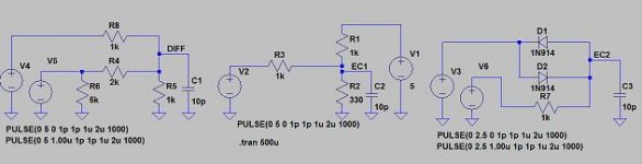
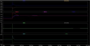
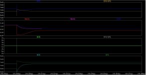
I did some playing around comparing some different level translator circuits for the 1541', assume the 10pf is the actuall input capacitance of the dac you can see how much is injected into it.
I think there might be room for some improvement with regard to the back to back diode solution.
Note tough the rise / fall times are intentionally set high (wich exacerbates things)
I think there might be room for some improvement with regard to the back to back diode solution.
Note tough the rise / fall times are intentionally set high (wich exacerbates things)
Attachments
TDA1387
Hi John,
Going back to the TDA1543 simple implementation, have you ever experimented with the TDA1387 or TDA1545(EIAJ)?
They are 8pin and simple as the TDA1543 but with the 0v output compliance of the TDA1541.
It could be better sounding than TDA1543 but less complicated than TDA1541 DAC.
Only use the input stage from TDA1543 schema and the output mosfet + 500r i/v stage of the TDA1541
TDA1387 is discontinued but can be found on all soundblaster awe64 and soundblaster 16 (CT2770)
I've been playing with all three varieties of 8-pin DACs you mentioned. Its quite a lot of hard work to get the TDA1545 and TDA1387 sound as good as the TDA1543, even though their measurements look better on paper. I take it because they're CMOS parts they play mean with their power supplies, whereas the 1543 being bipolar is fairly benign in this regard. Also the 1543's current source can be disabled whereas the others' cannot. TDA1387 is available on the second hand market here in China and extremely good bang for the buck at under 10cents a pop.
Hi roger57,
TDA1541A DEM oscillator is now soft-synced with 2.8224 MHz bit clock (attached picture). Sync signal is now taken from pin 2 (BCK) only.
The bit clock is derived from the masterclock using two UHS D flip-flops that form a synchronous divide-by-4 Johnson counter.
Both, new masterclock module and better performing DEM clock resulted in more transparency and more unmasked flaws.
....
The new voltage regulators and current buffers further increased transparency, now revealing resistor noise spectrum issues. Some critical resistors in volume control and Circlotron power amp had to be changed to hybrid resistors in order to fine-tune the system noise spectrum. The hybrid resistors consist of the right "mix" of bulk metal foil, carbon composition, metal film and wire-wound resistors.
EC Designs / John,
Thank you for the thorough response. I always wonder how you find the time to provide such answers to DIY members, and yet find the time to do all your design. Do you ever find time to sleep?

My present TDA1541A board uses an inverter from BCLK for the DEM clock input, which seems to be a good result. However, I was asking about the clocking circuit as I was actually going to build the Mk7 reclock circuit, but I guess that won't happen now, based on what you are saying. Also interested in your regulator specifics and what you have found there.
As with your previous designs, do you think you might post them here in the near future?
Regards,
Gary
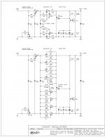
Hi roger57,
I attached schematics of common-mode shunt regulators I am currently experimenting with.
First diagram is the 3V6 shunt regulator for the sub miniature timing module. It is set @ 20mA. It consists of a common-mode ripple rejection circuit (T1, T2, R1, R2, C1...C3). This circuit provides a clean non-stabilized DC voltage.
Constant current sources are placed in feed and return lines, different types of CCS can be used here. The main function of these CCS is increasing impedance between load and transformer.
Regulator noise spectrum has big impact on sound quality, even if it's in the nanovolt range. I suspect this low level noise still manages to modulate masterclock and cause trigger uncertainty in logic circuits and D/A stage.
R3 and R5 (carbon composition resistors) are used as pink noise generators. Their signal is attenuated and summed to current sensing resistors R3 and R6. Regulator noise spectrum modulates the masterclock frequency. Since power supply noise cannot be reduced to zero, and the noise spectrum of power supply and masterclock combination may not be ideal, this noise spectrum tuning becomes necessary in order to approximate perfect tonal balance.
The shunt regulator is a straight-forward circuit consisting of a high gain Darlington (T6), filtered LED reference (L1, C4, and C5) and a temperature compensated transistor (T7).
The second shunt regulator is intended for TDA1541A +5V supply and low impedance reference voltage (DC-coupling), it is set @ 100mA. I used multiple JFET CCS in parallel here in order to achieve low voltage drop. It is also possible to use different CCS here, depending on input voltage / voltage drop.
Since these are "floating" supplies it is possible to connect them similar to batteries. This way the same circuit can be used for positive and negative power supplies.
The -15V shunt regulator has 2 LEDs in series and value for R24 is increased to approx. 3K.
The common mode ripple rejection circuit must be located as close to the transformer as possible in order to keep wiring carrying ripple / noise voltage as short as possible. This way ripple and interference is mainly concentrated on the mains power supply module.
The clean DC voltage is fed to the regulators using (shielded) twisted pairs. Shunt regulators must be placed as close to the load as possible, in order to achieve this they should be built as compact as possible, 10 x 20mm PCB for example. It is also desirable to fully screen the shunt regulator PCBs in order to maintain low noise levels (EMI).
Also interested in your regulator specifics and what you have found there.
I attached schematics of common-mode shunt regulators I am currently experimenting with.
First diagram is the 3V6 shunt regulator for the sub miniature timing module. It is set @ 20mA. It consists of a common-mode ripple rejection circuit (T1, T2, R1, R2, C1...C3). This circuit provides a clean non-stabilized DC voltage.
Constant current sources are placed in feed and return lines, different types of CCS can be used here. The main function of these CCS is increasing impedance between load and transformer.
Regulator noise spectrum has big impact on sound quality, even if it's in the nanovolt range. I suspect this low level noise still manages to modulate masterclock and cause trigger uncertainty in logic circuits and D/A stage.
R3 and R5 (carbon composition resistors) are used as pink noise generators. Their signal is attenuated and summed to current sensing resistors R3 and R6. Regulator noise spectrum modulates the masterclock frequency. Since power supply noise cannot be reduced to zero, and the noise spectrum of power supply and masterclock combination may not be ideal, this noise spectrum tuning becomes necessary in order to approximate perfect tonal balance.
The shunt regulator is a straight-forward circuit consisting of a high gain Darlington (T6), filtered LED reference (L1, C4, and C5) and a temperature compensated transistor (T7).
The second shunt regulator is intended for TDA1541A +5V supply and low impedance reference voltage (DC-coupling), it is set @ 100mA. I used multiple JFET CCS in parallel here in order to achieve low voltage drop. It is also possible to use different CCS here, depending on input voltage / voltage drop.
Since these are "floating" supplies it is possible to connect them similar to batteries. This way the same circuit can be used for positive and negative power supplies.
The -15V shunt regulator has 2 LEDs in series and value for R24 is increased to approx. 3K.
The common mode ripple rejection circuit must be located as close to the transformer as possible in order to keep wiring carrying ripple / noise voltage as short as possible. This way ripple and interference is mainly concentrated on the mains power supply module.
The clean DC voltage is fed to the regulators using (shielded) twisted pairs. Shunt regulators must be placed as close to the load as possible, in order to achieve this they should be built as compact as possible, 10 x 20mm PCB for example. It is also desirable to fully screen the shunt regulator PCBs in order to maintain low noise levels (EMI).
Attachments
Hi ecdesigns,
Interesting thread. Read till thread 70 and the last page 418. Hope to read the remaining pages soon. Might be my next building project. Keep up the good work.
A suggestion:
In post #4175 you mention a LED reference:
"The shunt regulator is a straight-forward circuit consisting of a high gain Darlington (T6), filtered LED reference (L1, C4, and C5) and a temperature compensated transistor (T7)." I suppose low frequency might give the most trouble.
An idea might be to replace the LED by a low noise NPN transistor used as a Zener with collecter lead clipped off, base connected to negative and emitter connected to positive voltage. This might result in better noise figures then LEDs with a main advantage in the lower frequency range. Example: BFP520. I haven't tried it myself yet, so no experience.
More interesting info about LED noise (maybe mentioned before?): http://www.diyaudio.com/forums/parts/35821-some-noise-measurements-leds-zener-diodes.html
Here is a photo of the sonic resonator, a 360 degree radiator with real-time correction system for sub-bass, bass and mid. This system needs no damping materials. Mid-high and High are placed in an open resonance chamber with conical deflectors and polarizer discs for incredible realistic sound, it actually reconstructs the acoustics of the place the recording was made, with pinpoint accuracy. Chesky audio recordings sound magnificent on these sonic resonators. The photo shows an early prototype of about 4 years ago. Components are handcrafted form MDF and sprayed with metallic paint. The new version has solid aluminum and plastic parts and is sonically optimized to the max. It has a highly optimized passive filter using some very exotic parts like NON-inductive stranded copper wire resistors (took a long time and many listening sessions to fine-tune). You cannot believe how much effect a simple component as a resistor, capacitor or coil can have on sound reproduction. As I already said, hearing is believing. The most common reaction I get from High-End enthousiasts is: this sound cannot possibly come from those speakers....but then, it does. Second is, where is the subwoofer? ,those speakers cannot produce that bass or can they... sure they can.
those speakers are too cool. would love to hear them
Hi John,
So, are you tuning the amount of pink noise generated by the regulator for the sonic impact, or what?
RFI/EMI propagate also by radiation, therefore, it seems to me that a good approach may be to filter them as much as possible, right at the mains entrance. Also, power transformer(s) with a static shield between the primary and secondary may be of a benefit. Also, bypassing (Zobel) the rectifier diodes and RF LC or CLC filter right after the rectifying diodes. It seems that there is never too much caution, or over-doing, when it concerns filtering RFI/EMI.
Regulator noise spectrum has big impact on sound quality, even if it's in the nanovolt range. I suspect this low level noise still manages to modulate masterclock and cause trigger uncertainty in logic circuits and D/A stage.
R3 and R5 (carbon composition resistors) are used as pink noise generators. Their signal is attenuated and summed to current sensing resistors R3 and R6. Regulator noise spectrum modulates the masterclock frequency. Since power supply noise cannot be reduced to zero, and the noise spectrum of power supply and masterclock combination may not be ideal, this noise spectrum tuning becomes necessary in order to approximate perfect tonal balance.
So, are you tuning the amount of pink noise generated by the regulator for the sonic impact, or what?
The common mode ripple rejection circuit must be located as close to the transformer as possible in order to keep wiring carrying ripple / noise voltage as short as possible. This way ripple and interference is mainly concentrated on the mains power supply module.
The clean DC voltage is fed to the regulators using (shielded) twisted pairs. Shunt regulators must be placed as close to the load as possible, in order to achieve this they should be built as compact as possible, 10 x 20mm PCB for example. It is also desirable to fully screen the shunt regulator PCBs in order to maintain low noise levels (EMI).
RFI/EMI propagate also by radiation, therefore, it seems to me that a good approach may be to filter them as much as possible, right at the mains entrance. Also, power transformer(s) with a static shield between the primary and secondary may be of a benefit. Also, bypassing (Zobel) the rectifier diodes and RF LC or CLC filter right after the rectifying diodes. It seems that there is never too much caution, or over-doing, when it concerns filtering RFI/EMI.
Hi Joshua_G,
The noise at the load cannot be reduced to zero at room temperature regardless of voltage regulator specs. This noise will have certain noise spectrum, and depending on this spectrum the noise can cause unacceptable degrading of perceived sound quality at these performance levels. Fine tuning this noise spectrum can improve perceived sound quality.
When using suitable ultra low noise pre-amp, noise spectrum tuning can be verified by a spectrum analyser.
Check schematics in post #4073, it shows the the filter circuits in the mains power supply.
I use multiple balanced LC filters to attenuate interference. The schematic also shows I am using Schottky diodes, these don't require Zobel networks.
Safety earth gets polluted because it runs along mains feed and return lines. Since the mains wires aren't twisted together but are usually simply placed in a plastic tube, interference on protective earth lead cannot be nulled. This means that when a static shield is connected to this polluted safety earth lead it can even inject more interference into the power supply this way. This of course depends on local conditions.
The reason a digital audio reproduction system is so extremely sensitive to noise is that system clock, bit clock and word clock act as carrier waves for lower frequency interference signals that are modulated on it by power supply, ground or digital audio source for example. We than have multiple FM / AM radio transmitters right on the DAC module that can spread interference over the entire DAC circuits where its locally demodulated. After demodulation we basically transported interference wirelessly from point A to point B.
In an analogue sound reproduction system we sometimes have problems with high frequency oscillation in the power amp. This usually results in audible hum and interference. This is a simple example how the interference (power supply ripple voltage) is modulated on a carrier wave (oscillating power amp) and then demodulated, feeding power supply ripple voltage to the speakers.
In analogue sound reproduction systems we can easily fix this problem by preventing oscillations that can then act as carrier wave. With digital audio reproduction systems we are stuck with the carrier waves and have to figure out different solutions.
So, are you tuning the amount of pink noise generated by the regulator for the sonic impact, or what?
The noise at the load cannot be reduced to zero at room temperature regardless of voltage regulator specs. This noise will have certain noise spectrum, and depending on this spectrum the noise can cause unacceptable degrading of perceived sound quality at these performance levels. Fine tuning this noise spectrum can improve perceived sound quality.
When using suitable ultra low noise pre-amp, noise spectrum tuning can be verified by a spectrum analyser.
RFI/EMI propagate also by radiation, therefore, it seems to me that a good approach may be to filter them as much as possible, right at the mains entrance. Also, power transformer(s) with a static shield between the primary and secondary may be of a benefit. Also, bypassing (Zobel) the rectifier diodes and RF LC or CLC filter right after the rectifying diodes. It seems that there is never too much caution, or over-doing, when it concerns filtering RFI/EMI.
Check schematics in post #4073, it shows the the filter circuits in the mains power supply.
I use multiple balanced LC filters to attenuate interference. The schematic also shows I am using Schottky diodes, these don't require Zobel networks.
Safety earth gets polluted because it runs along mains feed and return lines. Since the mains wires aren't twisted together but are usually simply placed in a plastic tube, interference on protective earth lead cannot be nulled. This means that when a static shield is connected to this polluted safety earth lead it can even inject more interference into the power supply this way. This of course depends on local conditions.
The reason a digital audio reproduction system is so extremely sensitive to noise is that system clock, bit clock and word clock act as carrier waves for lower frequency interference signals that are modulated on it by power supply, ground or digital audio source for example. We than have multiple FM / AM radio transmitters right on the DAC module that can spread interference over the entire DAC circuits where its locally demodulated. After demodulation we basically transported interference wirelessly from point A to point B.
In an analogue sound reproduction system we sometimes have problems with high frequency oscillation in the power amp. This usually results in audible hum and interference. This is a simple example how the interference (power supply ripple voltage) is modulated on a carrier wave (oscillating power amp) and then demodulated, feeding power supply ripple voltage to the speakers.
In analogue sound reproduction systems we can easily fix this problem by preventing oscillations that can then act as carrier wave. With digital audio reproduction systems we are stuck with the carrier waves and have to figure out different solutions.
Last edited:
- Home
- Source & Line
- Digital Line Level
- Building the ultimate NOS DAC using TDA1541A