Hello EC,
May I know whose I2S format are you using, Philips? From what I read at Lampizator website, Sony is using a different I2S format. Do we just follow the instructions at Lampizator website to convert the format?
Next, you got me very excited about your MK3. I am sure there already buyers around the world and some may had given some review on the forums. Will you please post some of the comments/ reviews that your customer had given to your latest masterpiece?
Does S1/ S2 grade sound better in this latest version?
The hybrid coupling cap that performs closest to DC coupling was composed by paralleling 2.2uF/250V Monacor MKT, 3.3uF/250V Monacor MKT and a 40pF Teflon trimmer (set to max. value).
Hi John,
does it have a specific reason, why you use two separate caps to get 5,5µF?
Isn´t it easyer to use one with 6,8µF or is this value to high?
With 2 x TDA1541A you simply duplicate the FET current buffer (one 2SK170-BL JFET and one 10K bias resistor for each DAC) and connect both drains of the JFETs to the I/V resistor. The full scale current now doubles to 8mA, so R = 2 / 0.008 = 250R.
You mean i need for every DAC a separate pair of 2SK170 and go with the drains parallel on the I/V resistor?
Could´t i parallel the inputs at the source on one pair 2SK170?
Best,
Oliver
Last edited:
Hi dvb-projekt,
Major problem with coupling caps is the mechanical resonance of the charged foil and the effect (distortion) it introduces.
Then there is the problem of charge reversals at higher frequencies.
So I use two capacitors of same brand and type, but different value (2.2uF and 3.3uF). When placed in parallel these create a larger cap value with same properties, but each cap resonates at different frequencies because one is larger than the other. In practice this results in "mutual damping" of mechanical foil resonances in both caps. This leads to a cleaner sound (less distortion). The 40pF Teflon trimmer is used for fast charge reversals at high frequencies, and the teflon foil and plate construction ensures very low mechanical resonances.
In order to speed-up burn in process, each cap is subjected to a sweep signal (20 Hz ... 20 KHz) for approx. 24 hours. This "settles" the foil (mechanical resonance) by spreading the foil tension that builds-up during manufacturing.
At the start of the burn in process the caps can make quite some noise like small speakers, this reduces after burn in, so the effect can be verified.
The result is a hybrid coupling cap that offers close to DC performance for under eur 10 per cap.
Despite common preference for polypropylene caps, these specific Monacor MKT caps offered closest match with DC-coupling (I used a switch for immediate comparison with DC-coupling).
I don't use full DC-coupling in my set (although this would be possible) for safety reasons. When for some reason the bit clock stops, I could end up with 40V DC on my speakers. The single coupling cap in the entire signal path prevents this.
Yes, this ensures low impedance at each DAC output. If only one JFET for all 4 DAC chips is used, impedance at DAC chip outputs wouldn't be low enough. The JFETs are used as impedance converters (low input impedance, high output impedance). This helps to minimize ac voltage at the DAC output while using large passive I/V resistor values.
does it have a specific reason, why you use two separate caps to get 5,5µF?
Isn´t it easier to use one with 6,8µF or is this value to high?
Major problem with coupling caps is the mechanical resonance of the charged foil and the effect (distortion) it introduces.
Then there is the problem of charge reversals at higher frequencies.
So I use two capacitors of same brand and type, but different value (2.2uF and 3.3uF). When placed in parallel these create a larger cap value with same properties, but each cap resonates at different frequencies because one is larger than the other. In practice this results in "mutual damping" of mechanical foil resonances in both caps. This leads to a cleaner sound (less distortion). The 40pF Teflon trimmer is used for fast charge reversals at high frequencies, and the teflon foil and plate construction ensures very low mechanical resonances.
In order to speed-up burn in process, each cap is subjected to a sweep signal (20 Hz ... 20 KHz) for approx. 24 hours. This "settles" the foil (mechanical resonance) by spreading the foil tension that builds-up during manufacturing.
At the start of the burn in process the caps can make quite some noise like small speakers, this reduces after burn in, so the effect can be verified.
The result is a hybrid coupling cap that offers close to DC performance for under eur 10 per cap.
Despite common preference for polypropylene caps, these specific Monacor MKT caps offered closest match with DC-coupling (I used a switch for immediate comparison with DC-coupling).
I don't use full DC-coupling in my set (although this would be possible) for safety reasons. When for some reason the bit clock stops, I could end up with 40V DC on my speakers. The single coupling cap in the entire signal path prevents this.
You mean i need for every DAC a separate pair of 2SK170 and go with the drains parallel on the I/V resistor?
Yes, this ensures low impedance at each DAC output. If only one JFET for all 4 DAC chips is used, impedance at DAC chip outputs wouldn't be low enough. The JFETs are used as impedance converters (low input impedance, high output impedance). This helps to minimize ac voltage at the DAC output while using large passive I/V resistor values.
Hi fff0,
I use Philips I2S, 32 bits / frame, meaning 16 bits of L channel immediately followed by 16 bits of R channel and so on. This turned out to offer lowest interference levels compared to 64 bits / frame I2S. Other advantage of I2S 32 bits / frame is that I could go up to 192 / 16 with the TDA1541A.
The MK3 version is brand new so I have to wait a little while for reviews. There are some forum members that can test this MK3 version soon (modified units have just been shipped), It would be nice if they would like share their experiences with this new module.
This depends on manufacturing date, the newest TDA1541A usually sound best. I even got some plain A versions manufactured in '98 that outperform S1 versions from '88. This can be explained by improved production techniques (and resulting higher accuracy / lower bit errors).
The best TDA1541A would be a S2 of most recent production, but these are quite rare and very expensive.
May I know whose I2S format are you using, Philips? From what I read at Lampizator website, Sony is using a different I2S format. Do we just follow the instructions at Lampizator website to convert the format?
I use Philips I2S, 32 bits / frame, meaning 16 bits of L channel immediately followed by 16 bits of R channel and so on. This turned out to offer lowest interference levels compared to 64 bits / frame I2S. Other advantage of I2S 32 bits / frame is that I could go up to 192 / 16 with the TDA1541A.
Next, you got me very excited about your MK3. I am sure there already buyers around the world and some may had given some review on the forums. Will you please post some of the comments/ reviews that your customer had given to your latest masterpiece?
The MK3 version is brand new so I have to wait a little while for reviews. There are some forum members that can test this MK3 version soon (modified units have just been shipped), It would be nice if they would like share their experiences with this new module.
Does S1/ S2 grade sound better in this latest version?
This depends on manufacturing date, the newest TDA1541A usually sound best. I even got some plain A versions manufactured in '98 that outperform S1 versions from '88. This can be explained by improved production techniques (and resulting higher accuracy / lower bit errors).
The best TDA1541A would be a S2 of most recent production, but these are quite rare and very expensive.
I don't use full DC-coupling in my set (although this would be possible) for safety reasons. When for some reason the bit clock stops, I could end up with 40V DC on my speakers. The single coupling cap in the entire signal path prevents this.
I am running my Horn´s with a 300B SET from Triode Dick (Ceasar II). If i am not wrong i don´t have any problems with DC coupling, so i could forget the caps, right?
1541a-mk3
my short first feedback regarding the sd-player 1541a-mk3:
http://www.diyaudio.com/forums/digital-source/140538-lossless-sd-card-player-61.html#post2279451
cheers
mamal
my short first feedback regarding the sd-player 1541a-mk3:
http://www.diyaudio.com/forums/digital-source/140538-lossless-sd-card-player-61.html#post2279451
cheers
mamal
Guys, I need help ...
I'm new here, I want to build DAC using TDA1541 or 1541A, I wonder if you can help me, at least point me which KIT is worth the money ?
budget is less than US$150,-. (no 1541)
possible ?
there are so many Kit's available, specially on ebay.
don't know which one is better or worth the money.
and I don't this I can read this thread with 300+ pages....
so please point me on the right direction or which KIT is good/best for the money ?
and there are many fake 1541a, I wonder if the oroginal still available ? howmuch ?
Best regards
Cal
Guys, I need help ...
I'm new here, I want to build DAC using TDA1541 or 1541A, I wonder if you can help me, at least point me which KIT is worth the money ?
budget is less than US$150,-. (no 1541)
possible ?
there are so many Kit's available, specially on ebay.
don't know which one is better or worth the money.
and I don't this I can read this thread with 300+ pages....
so please point me on the right direction or which KIT is good/best for the money ?
and there are many fake 1541a, I wonder if the oroginal still available ? howmuch ?
Best regards
Cal
How about this one ?
DAC TDA1541A+WM8805 OS & NOS 1.0U multi-input - eBay (item 320577335097 end time Aug-27-10 09:15:40 PDT)
Have you built this one ?
how is the SQ ? compare to what ?
Cal
how is the SQ ? compare to what ?
Cal
Limiting Bandwidth
John,
In your post #3415 you propose a new 'I2S attenuator'.
1. What are the benefits to this one in comparison to the earlier version?
2. There are many 'knowlegable' people, that in different threads on this forum, has talked about limiting the bandwidth, risetime of the clock edges. There is no use in clocking an input with a faster risetime than the receiving logic can handle, you just increase noise and inject excess current leading to groundbounce. What are your finding in this area? (You are always talking about ground bounce, but this seems a bit contradictory to me in the latest circuit?)
3. In simulation, your latest 'I2S attenuator' circuit gives current spikes on the input. Anything you have seen in the real world?
Keep up you fantastic work !
Per
Have you built this one ?
how is the SQ ? compare to what ?
Cal
I have not built this one.
Hi phi,
There is a paradox, on one hand we need fastest positive transients (TDA154x output register triggers on positive transient of BCK) in order to minimize trigger uncertainty (and relating jitter). On the other hand we need slower transients to reduce the effects of ground-bounce. Like with most things, it looks we have to make a compromise.
Ok, I will try to explain I2S attenuator (and attached TDA154x input circuit) in detail.
Starting with TDA154x I2S input, it consists of a current source feeding 3 diodes that are placed in series. The junction between current source and anode of first diode is connected to the input pin through another diode, cathode facing the input pin. Input stray capacitance is specified at 15pF. The current steering logic is connected to the junction of current source and anode of the diode. You can find these specs and on-chip I2S input circuit schematics in the TDA1543 / TDA1541A data sheets.
Trigger level is typically 3 * 0.6V (3 diodes in series) minus 0.6V (input diode) equals approx. 1.2V, this trigger threshold varies slightly with chip temperature (diodes).
What I did was minimizing signal amplitude and providing 0.6V bias voltage level (this reduces ground-bounce). Positive transients are fast, negative transients are band-limited by a 1K resistor that is part of the new I2S attenuator. Furthermore I prevented simultaneous switching of I2S and DEM signals, this further reduces ground-bounce.
Input = 0, /Q supplies +2.4V through 1K resistor. Q = 0V and pulls 2.4V down to 0.6V by diode 1. Result: 15pF is discharged from 1.8V to 0.6V through 1K / 15pF RC filter (band limiting).
Input = 1, /Q output places 1K in parallel with 15pF, Q charges 15pF through D2 as fast as possible, max. amplitude equals 2.4-0.6 = 1.8V.
So we have fast positive transient from 0.6 to 1.8V and slow (band limited) negative transient from 1.8 to 0.6V.
In order to further minimize ground-bounce on the critical positive transient of BCK, DATA, WS and DEM signal transients are phase shifted to prevent simultaneous switching (and related increased ground-bounce).
Diodes D1 and D2 provide some compensation for temperature changes as well, ensuring reliable operation.
In your post #3415 you propose a new 'I2S attenuator'.
1. What are the benefits to this one in comparison to the earlier version?
2. There are many 'knowlegable' people, that in different threads on this forum, has talked about limiting the bandwidth, risetime of the clock edges. There is no use in clocking an input with a faster risetime than the receiving logic can handle, you just increase noise and inject excess current leading to groundbounce. What are your finding in this area? (You are always talking about ground bounce, but this seems a bit contradictory to me in the latest circuit?)
3. In simulation, your latest 'I2S attenuator' circuit gives current spikes on the input. Anything you have seen in the real world?
There is a paradox, on one hand we need fastest positive transients (TDA154x output register triggers on positive transient of BCK) in order to minimize trigger uncertainty (and relating jitter). On the other hand we need slower transients to reduce the effects of ground-bounce. Like with most things, it looks we have to make a compromise.
Ok, I will try to explain I2S attenuator (and attached TDA154x input circuit) in detail.
Starting with TDA154x I2S input, it consists of a current source feeding 3 diodes that are placed in series. The junction between current source and anode of first diode is connected to the input pin through another diode, cathode facing the input pin. Input stray capacitance is specified at 15pF. The current steering logic is connected to the junction of current source and anode of the diode. You can find these specs and on-chip I2S input circuit schematics in the TDA1543 / TDA1541A data sheets.
Trigger level is typically 3 * 0.6V (3 diodes in series) minus 0.6V (input diode) equals approx. 1.2V, this trigger threshold varies slightly with chip temperature (diodes).
What I did was minimizing signal amplitude and providing 0.6V bias voltage level (this reduces ground-bounce). Positive transients are fast, negative transients are band-limited by a 1K resistor that is part of the new I2S attenuator. Furthermore I prevented simultaneous switching of I2S and DEM signals, this further reduces ground-bounce.
Input = 0, /Q supplies +2.4V through 1K resistor. Q = 0V and pulls 2.4V down to 0.6V by diode 1. Result: 15pF is discharged from 1.8V to 0.6V through 1K / 15pF RC filter (band limiting).
Input = 1, /Q output places 1K in parallel with 15pF, Q charges 15pF through D2 as fast as possible, max. amplitude equals 2.4-0.6 = 1.8V.
So we have fast positive transient from 0.6 to 1.8V and slow (band limited) negative transient from 1.8 to 0.6V.
In order to further minimize ground-bounce on the critical positive transient of BCK, DATA, WS and DEM signal transients are phase shifted to prevent simultaneous switching (and related increased ground-bounce).
Diodes D1 and D2 provide some compensation for temperature changes as well, ensuring reliable operation.
And yes, the I2S attenuator circuit does make a significant improvement in sound...as does the excellent DIY honeycomb I/V resistors. ")
I remember the clues for the I2S attenuator were posted here years ago by a Philips ingeneer but only -EC- develloped a working solution, to our benefit.
Cheers,
M.
I remember the clues for the I2S attenuator were posted here years ago by a Philips ingeneer but only -EC- develloped a working solution, to our benefit.
Cheers,
M.
Thank's a lot for your thorough reply John !
Yes it's a bit of a paradox with noise, slew rate and jitter and I must admit that I have not really grasped it.
You want fastest possible slew rate to minimize unsertainty, but that increases bandwidth, noise level and ground bounce.
As you say, everthing is a compromize and the components available will decide what you can achieve.
Was it a big difference changing to this new I2S-attenuator?
Which implementation are you refering to maxlorenz ?
Per
Last edited:
Hi,
I try to follow always the circuit posted by -ECdesigns- as is.
I have made some attenuators with variable resistors to fit different I2S sources, but since I am now lacking a scope, it is a bit risky.
It's no risk of to much attenuation. It just won't work.
But how one can fiddle with this without a scope is beyond my imagination. You just can't verify anything, can you?
Also, It's very hard to follow all of -ecdesigns- "findings" and "wow's" in all versions of the same circuit, so you need a scope to be really confident on what you do and achieve. Buy a scope and extend your hobby.

I did a attenuator and verified it and also use it... but I can't say I heard any difference. Something most of the DIY nerds here wouldn't admit, would they
To take your pants of in public and say you don't hear things everyone else does, ha ha.
Hi EC,
Have you seen the following implemention suggestion of LC network before a regulator?
Improved Power Supply Rejection For IC Linear Regulators - Maxim
Have you seen the following implemention suggestion of LC network before a regulator?
Improved Power Supply Rejection For IC Linear Regulators - Maxim
Hi Radioman62,
There is another thread about I2S attenuators, information about this subject is provided by Henk ten Pierick who seems to have contacts to people involved in TDA1541A chip development at former Philips Eindhoven.
All I can say is that the theoretical reason for using such circuits is reduction of ground-bounce at the I2S input circuit. This in turn leads to lower on-chip jitter. On-chip jitter introduces highest jitter levels followed by reclockers and masterclock. Therefore it is very important to achieve lowest possible on-chip jitter. Other reason for minimizing I2S induced interference is keeping DAC analogue outputs as clean as possible (on-chip crosstalk).
The audibility of the reduced on-chip jitter levels also depends on resolution of DAC output circuit and connected audio equipment. If these have too low resolution, the effect of such I2S attenuator might not be audible. One also needs to know what effects to listen for, the lower I2S interference levels in general lead to darker background and audible effects related to lower jitter levels.
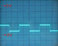
Most applications simply dump 5Vpp TTL signals on the TDA1541x I2S inputs, resulting in maximum ground-bounce. My latest diode resistor I2S attenuators output a signal that varies between approx. +0.6V and +1.8V. I attached an oscillogram showing BCK signal. I added markers for GND and +5V levels.
I use fast synchronous reclockers on all I2S signals. I didn't divide the masterclock by 8 and 256 to derive BCK and WS because this would require 11 flip-flops that would need to switch synchronous, thus causing significant ground-bounce. This in turn would prevent achieving lowest possible jitter levels on all I2S signals. The synchronous reclocker alternative only requires 3 flip-flops, only 2 of these are triggered at the same moment to further minimize ground-bounce.
I did a attenuator and verified it and also use it... but I can't say I heard any difference. Something most of the DIY nerds here wouldn't admit, would they
To take your pants of in public and say you don't hear things everyone else does, ha ha.
There is another thread about I2S attenuators, information about this subject is provided by Henk ten Pierick who seems to have contacts to people involved in TDA1541A chip development at former Philips Eindhoven.
All I can say is that the theoretical reason for using such circuits is reduction of ground-bounce at the I2S input circuit. This in turn leads to lower on-chip jitter. On-chip jitter introduces highest jitter levels followed by reclockers and masterclock. Therefore it is very important to achieve lowest possible on-chip jitter. Other reason for minimizing I2S induced interference is keeping DAC analogue outputs as clean as possible (on-chip crosstalk).
The audibility of the reduced on-chip jitter levels also depends on resolution of DAC output circuit and connected audio equipment. If these have too low resolution, the effect of such I2S attenuator might not be audible. One also needs to know what effects to listen for, the lower I2S interference levels in general lead to darker background and audible effects related to lower jitter levels.
Most applications simply dump 5Vpp TTL signals on the TDA1541x I2S inputs, resulting in maximum ground-bounce. My latest diode resistor I2S attenuators output a signal that varies between approx. +0.6V and +1.8V. I attached an oscillogram showing BCK signal. I added markers for GND and +5V levels.
I use fast synchronous reclockers on all I2S signals. I didn't divide the masterclock by 8 and 256 to derive BCK and WS because this would require 11 flip-flops that would need to switch synchronous, thus causing significant ground-bounce. This in turn would prevent achieving lowest possible jitter levels on all I2S signals. The synchronous reclocker alternative only requires 3 flip-flops, only 2 of these are triggered at the same moment to further minimize ground-bounce.
Attachments
Hi fff0,
Yes I already studied these applications, and yes I use a RC filter (well sort of) in front of all regulators used in the TDA1541A DAC module.
Instead of using lossy RC filters I used capacitance multipliers that pre-filter the unregulated input voltage prior to feeding it to the voltage regulators. This way the regulators basically get a clean unregulated DC input voltage.
I also added RF / HF filters between capacitance multiplier and voltage regulator and between voltage regulator and loads.
Highly sensitive circuits like masterclock and synchronous bit reclocker are connected through an additional 6 ... 12th order LC filter placed after the voltage regulator.
I also experimented with cascaded regulators (used in octal D-I DAC and DI8M), but the primary regulator feeds large bandwidth noise into the secondary regulator that has limited bandwidth (like the primary regulator). So this isn't optimal either.
Apart form providing clean power supply, it is best to construct connected circuits such way that these have highest possible PSRR.
Have you seen the following implemention suggestion of LC network before a regulator?
Yes I already studied these applications, and yes I use a RC filter (well sort of) in front of all regulators used in the TDA1541A DAC module.
Instead of using lossy RC filters I used capacitance multipliers that pre-filter the unregulated input voltage prior to feeding it to the voltage regulators. This way the regulators basically get a clean unregulated DC input voltage.
I also added RF / HF filters between capacitance multiplier and voltage regulator and between voltage regulator and loads.
Highly sensitive circuits like masterclock and synchronous bit reclocker are connected through an additional 6 ... 12th order LC filter placed after the voltage regulator.
I also experimented with cascaded regulators (used in octal D-I DAC and DI8M), but the primary regulator feeds large bandwidth noise into the secondary regulator that has limited bandwidth (like the primary regulator). So this isn't optimal either.
Apart form providing clean power supply, it is best to construct connected circuits such way that these have highest possible PSRR.
- Home
- Source & Line
- Digital Line Level
- Building the ultimate NOS DAC using TDA1541A