
Standing current.
Hi Omainik
Are you running in balanced or unbalanced mode?
What are you doing with the 8ma standing current of 4 tda1541A's ? (Sowter rated only for 0.6 standing current). If they are fed through the transformer primary, they would give quite some bias voltage because of the primary's DCR.
Regards
Martin
Hi Martin,
the current flows through the primary. I can't detect audible side effects.
recently I compared 4 parallel DAC with one single DAC. With no DEM clock injection there is a difference. With injected DEM clock there is no audible difference for me between 4 and 1 dac.
best regards
peter
the current flows through the primary. I can't detect audible side effects.
recently I compared 4 parallel DAC with one single DAC. With no DEM clock injection there is a difference. With injected DEM clock there is no audible difference for me between 4 and 1 dac.
best regards
peter
Please forgive me for asking a basic question, but I'd like to use the charge transfer circuit to provide the raw DC to a simple dual voltage regulator. It's based on a LM317/337, and is set up to provide +12Vdc and -12Vdc.
At the moment it is fed by a transformer, with the centre tap on a common line to the 0v of the DC output, and the AC feeding the rectifiers, which then supply the regulators.
If I use the Charge Transfer Circuit in post 2579, would I connect the + output of the charge transfer to the input of the LM317, and the - output to the input of the LM337. The transformer center tap would not be connected, but the 0v output would still be at 0v, as it is in relation to the +/- 12Vdc output?
I hope this makes sense as I'm pretty new to electronics (started learning and reading 4 months ago!) and have found a world of joy here!
Hi Isiitoolate,
Since there are no answers yet I will try to respond. Be aware that I am no EE...
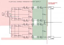
You are referring to the so called floating CT supply, which at first glance is more difficult to use in your application than the non floating, original version.
As the diagram shows, the TX center tap must be connected to the midpoint between C1 and C2. If you use positive output of the CTS to the input of 317 you can use this midpoint as ground. The same for the negative output, but this will negate the effect of the floating approach, I imagine...
Please be aware that the floating CTS has almost the complete voltage that the TX is able to give between the pos and neg output, and that C3 will see this V, so you have to check out if it is rated for that V (you have not mentioned what VAC are your TX secondaries, BTW).
If you use the negative out as ground for positive out the power dissipation in you 317reg could be high.
The second way I see that this supply could work, but I have not tested it, is making a double connection for pos out and for neg out> one pos out is the real pos out and the other is ground for the neg rail...I don-t know if I made myself clear...this should keep it floating...but the regs will see the whole V and will waste more heat...I wish EC was around to contrast this hypothesis.
Edit> you could also replace C3 by two caps in series and take the midpoint of this cap arrangement as you 0V! ...maybe you must add R in parallel to each of these C to have exactly the electric midpoint? This arrangement will divide by two the rated capacitance though...opinions please.
I hope this hepls,
Regards and congratulations to decide to try these PS> you won-t regret it.
I use them everywhere!
M
Since there are no answers yet I will try to respond. Be aware that I am no EE...
You are referring to the so called floating CT supply, which at first glance is more difficult to use in your application than the non floating, original version.
As the diagram shows, the TX center tap must be connected to the midpoint between C1 and C2. If you use positive output of the CTS to the input of 317 you can use this midpoint as ground. The same for the negative output, but this will negate the effect of the floating approach, I imagine...
Please be aware that the floating CTS has almost the complete voltage that the TX is able to give between the pos and neg output, and that C3 will see this V, so you have to check out if it is rated for that V (you have not mentioned what VAC are your TX secondaries, BTW).
If you use the negative out as ground for positive out the power dissipation in you 317reg could be high.
The second way I see that this supply could work, but I have not tested it, is making a double connection for pos out and for neg out> one pos out is the real pos out and the other is ground for the neg rail...I don-t know if I made myself clear...this should keep it floating...but the regs will see the whole V and will waste more heat...I wish EC was around to contrast this hypothesis.
Edit> you could also replace C3 by two caps in series and take the midpoint of this cap arrangement as you 0V! ...maybe you must add R in parallel to each of these C to have exactly the electric midpoint? This arrangement will divide by two the rated capacitance though...opinions please.
I hope this hepls,
Regards and congratulations to decide to try these PS> you won-t regret it.
I use them everywhere!
M
Last edited:
Hi Maxlorenz,
Thanks for you thoughts, I really appreciate it. The transformer secondary Vac is twin 9Vac. This'll give 18Vac into the Charge Transfer circuit, and I hazard a guess of 20Vdc-ish after rectification. I'm guessing that C3 should be rated around 25-35Vdc?
I understand what you are saying about 'splitting' C3 in half, and having two 1500uF in series (although the circuit would see 700uF across the +/- rails?), but I cannot grasp your first suggestion (my fault!) Is it possible that you could do a diagram?
I'm a bit concerned about being OT (although the charge transfer appeared here), so apologies if this is the case.
Hi Isittoolate,
Build two FCT power supplies like in the schematics and connect them in series. Use two transformers or a transformer with separate secondary windings
FCT #1, plus positive supply voltage, minus ground.
FCT #2, plus ground, minus negative supply voltage.
Transformer center tap must not be connected as this would prevent creating a floating output voltage.
The idea is to isolate the load from the mains, avoiding / reducing the effects of (capacitive) ground loops and interference.
Unfortunately, the best isolation is obtained using battery power supply. This offers a true floating power supply and resulting performance will be accordingly. The improvements are most clearly noticed in upper mid-range and trebles.
Other option is to use mains power supply for one audio device only (power amp for example), and use battery power supply for the remaining equipment (source, DAC, volume control). This prevents creating (capacitive) ground loops too.
If I use the Charge Transfer Circuit in post 2579, would I connect the + output of the charge transfer to the input of the LM317, and the - output to the input of the LM337. The transformer center tap would not be connected, but the 0v output would still be at 0v, as it is in relation to the +/- 12Vdc output?
Build two FCT power supplies like in the schematics and connect them in series. Use two transformers or a transformer with separate secondary windings
FCT #1, plus positive supply voltage, minus ground.
FCT #2, plus ground, minus negative supply voltage.
Transformer center tap must not be connected as this would prevent creating a floating output voltage.
The idea is to isolate the load from the mains, avoiding / reducing the effects of (capacitive) ground loops and interference.
Unfortunately, the best isolation is obtained using battery power supply. This offers a true floating power supply and resulting performance will be accordingly. The improvements are most clearly noticed in upper mid-range and trebles.
Other option is to use mains power supply for one audio device only (power amp for example), and use battery power supply for the remaining equipment (source, DAC, volume control). This prevents creating (capacitive) ground loops too.
Hi jusbe,
I still have PCBs and some parts for the DI DAC projects in stock.
The DI DAC project was put on hold due to problems with digital audio sources (bit-perfect playback, interference, jitter, mechanical noise, and power consumption). If the digital audio source is already flawed, one cannot expect to achieve ultimate performance, not even with the most advanced DACs.
Most digital audio sources fail to provide bit-perfect playback by default. Computer-based digital audio sources often require extensive and repetitive tweaking (software updates). There are even some CD players / transports that fail to provide bit perfect playback (digital volume control). Interference present in the digital audio source will translate to jitter on the digital audio signals. So even a Toslink interface can transport digital audio source interference in the form of jitter / jitter spectrum. If the electronics in the DAC fail to completely block this jitter, it means source interference will still end up in the audio signal.
It would help a lot if the digital audio source would offer guaranteed bit-perfect playback and a cleaner digital signal (containing less interference / jitter) to start with. That way it's easier to achieve required low jitter / interference levels at the DAC.
Other problems relate to digital transmitter, interlink, and digital receiver. Usually SPDIF or USB are used to transport the digital audio data between source and DAC. Since these digital interfaces have known flaws, using them means making compromises.
In order to avoid these compromises in the first place, it's best to not use these digital audio interfaces at all (if possible), but this means integrating both digital audio source and DAC, using DAC chip digital interface like I2S for example.
So it would be beneficial to integrate both digital audio source and DAC while making sure the digital audio source provides cleanest possible signal (extreme low jitter / interference).
This resulted in designing a digital audio source from scratch, the lossless SD-player (semiconductor memory -based digital audio source).
The digital audio data is stored on a SD/HC memory card without compression using WAV format, this way the data remains transparent and exactly matches with the data on a CD. Interference produced during conversion (FLAC > WAV) that requires increased processing power is avoided. The data stored on the SD/HC card is output in the form of a I2S signal. The trick is to keep processor interference as low as possible, this was done using a low-power processor (nanowatt technology) that only consumes approx. 250mW under full load.
The clock signals were derived from a single ultra low jitter master clock that uses 3 selected / matched crystals. In order to maintain extreme low jitter levels, clock loads were reduced to only 2, and clock buffers weren't used as these would add extra jitter. One clock load is formed by the processor. The second is a high-speed flip-flop that synchronously reclocks the already low jitter BCK signal (I2S) from the processor. This method turned out to work better (lower jitter) than using a synchronous divider. The ultra low jitter clock then enters a dynamic jitter attenuator that further reduces the effects of jitter on sample timing.
I2S usually holds 64 bits/frame, 32 for L channel and 32 for R channel, but when using 16 bits for each channel only, 16 bits remain unused and have to be set to some value, usually zero. This then results in repetitive pulse bursts of 16 bits containing digital audio data and 16 bits containing zero. This will introduce interference (asymmetrical signal). In order to avoid this, the SD-player uses 32 bits/frame, 16 bits of L channel, immediately followed by 16 bits of R channel, creating a more symmetrical signal. Other advantage of this method is that bit clock could be lowered to absolute minimum value for 44.1/16 I2S namely 1.4112 MHz.
As stated before, the DAC is now integrated with the source and is directly connected through I2S, avoiding SPDIF/USB "issues".
Passive I/V conversion (resistor only) was used to completely avoid distortion produced by active devices.
In order to achieve lowest possible interference, very low noise power supplies had to be used. These consist of a battery power supply followed by low pass filters and voltage regulators. Noise levels then drop well below 205dB.
The SD-player is now completed and performs beyond expectation, in fact it performed so well that it revealed flaws in my audio set, forcing me to redesign volume control, power amplifiers and speakers before continuing. This took quite some time.
Volume control is a plain high quality potentiometer, relay contacts (depends on properties) will add subtle distortion, so the relay volume controls could no longer be used.
The MOSFET power amplifier failed to provide required resolution (low volume settings), so I designed a straight-forward, fully DC-coupled all-FET balanced bridge power amplifier. This amplifier has no global feedback, no constant current sources, no current mirrors nor DC-servo. The schematic is very simple (4 JFETs, 4 power MOSFETs, some resistors, few diodes, and a straight forward power supply (rectifier + smoothing caps). The amplifier accepts both balanced and single-ended input signals. Gain is rather high (bridge configuration) approx. 100x.
The 3-way speakers (omnidirectional, and based on the sonic resonator system) turned out to be limiting performance too. I now developed a new semi 2-way system that performs much better.
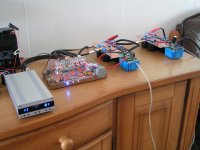
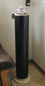
I attached a picture of the new prototype setup and new sonic resonator. It's a messy prototype setup for testing only.
So now I can finally continue with TDA1541A-based DAC development. needless to say that this DAC has to be driven by a SD-player using SD/HC memory cards.
The surrounding circuits for the TDA1541A were already discussed on this thread. I plan to use I2S attenuators, LED voltage regulators for +5V, -5V, and -15V, the latest DEM clock circuit (referenced to -15V using level translator). The decoupling caps (100nF) will be located underneath the chip for shortest possible connections.
I plan to use balanced output configuration, and since my power amplifier has relatively high gain, I could get away with true passive I/V conversion without any active components, producing say 300mVpp on each output. I plan to achieve this with the split I/V resistor circuit that includes a small bias current for manipulating TDA1541A output compliance, this way up to 550mVpp can be generated at the DAC outputs, maintaining low distortion. Combined I/V resistor value for each of the 4 outputs will need to be approx. 0.3 / 0.004 = 75 Ohms, so I could settle for 2 x 39 Ohms. This will also provide low output impedance.
The signal would then enter a quad volume potentiometer, and would be fed to the balanced inputs of the power amps. This way there is only one active circuit (power amplifier) between DAC output and speakers. Depending on DAC DC offset trimming I could get away with a fully DC-coupled system (no coupling caps at all). This would help to further reduce distortion.
So the ultimate NOS DAC project will probably result in a lossless SD-player with integrated, highly optimized TDA1541A-based DAC in dual mono configuration (requires 2 x TDA1541A/S1/S2).
About the interpolation (4x, 8x, 16x) used in earlier designs, this is no longer required when the digital audio source is virtually perfect (extreme low noise and jitter) and the connected audio equipment is able to handle the resulting unfiltered signal (audio spectrum plus reflected mirror images). Required brickwall filtering at approx. 20KHz will now be performed by the human auditory system. Just for clarity, I use no analogue filtering at all, except for the passive crossover filter in the speakers and the mechanical limitations of the speaker chassis.
Are you still selling this DAC? I've tried to reach you via your site but haven't heard from you and I wondered what was happening with it at the moment?
I still have PCBs and some parts for the DI DAC projects in stock.
The DI DAC project was put on hold due to problems with digital audio sources (bit-perfect playback, interference, jitter, mechanical noise, and power consumption). If the digital audio source is already flawed, one cannot expect to achieve ultimate performance, not even with the most advanced DACs.
Most digital audio sources fail to provide bit-perfect playback by default. Computer-based digital audio sources often require extensive and repetitive tweaking (software updates). There are even some CD players / transports that fail to provide bit perfect playback (digital volume control). Interference present in the digital audio source will translate to jitter on the digital audio signals. So even a Toslink interface can transport digital audio source interference in the form of jitter / jitter spectrum. If the electronics in the DAC fail to completely block this jitter, it means source interference will still end up in the audio signal.
It would help a lot if the digital audio source would offer guaranteed bit-perfect playback and a cleaner digital signal (containing less interference / jitter) to start with. That way it's easier to achieve required low jitter / interference levels at the DAC.
Other problems relate to digital transmitter, interlink, and digital receiver. Usually SPDIF or USB are used to transport the digital audio data between source and DAC. Since these digital interfaces have known flaws, using them means making compromises.
In order to avoid these compromises in the first place, it's best to not use these digital audio interfaces at all (if possible), but this means integrating both digital audio source and DAC, using DAC chip digital interface like I2S for example.
So it would be beneficial to integrate both digital audio source and DAC while making sure the digital audio source provides cleanest possible signal (extreme low jitter / interference).
This resulted in designing a digital audio source from scratch, the lossless SD-player (semiconductor memory -based digital audio source).
The digital audio data is stored on a SD/HC memory card without compression using WAV format, this way the data remains transparent and exactly matches with the data on a CD. Interference produced during conversion (FLAC > WAV) that requires increased processing power is avoided. The data stored on the SD/HC card is output in the form of a I2S signal. The trick is to keep processor interference as low as possible, this was done using a low-power processor (nanowatt technology) that only consumes approx. 250mW under full load.
The clock signals were derived from a single ultra low jitter master clock that uses 3 selected / matched crystals. In order to maintain extreme low jitter levels, clock loads were reduced to only 2, and clock buffers weren't used as these would add extra jitter. One clock load is formed by the processor. The second is a high-speed flip-flop that synchronously reclocks the already low jitter BCK signal (I2S) from the processor. This method turned out to work better (lower jitter) than using a synchronous divider. The ultra low jitter clock then enters a dynamic jitter attenuator that further reduces the effects of jitter on sample timing.
I2S usually holds 64 bits/frame, 32 for L channel and 32 for R channel, but when using 16 bits for each channel only, 16 bits remain unused and have to be set to some value, usually zero. This then results in repetitive pulse bursts of 16 bits containing digital audio data and 16 bits containing zero. This will introduce interference (asymmetrical signal). In order to avoid this, the SD-player uses 32 bits/frame, 16 bits of L channel, immediately followed by 16 bits of R channel, creating a more symmetrical signal. Other advantage of this method is that bit clock could be lowered to absolute minimum value for 44.1/16 I2S namely 1.4112 MHz.
As stated before, the DAC is now integrated with the source and is directly connected through I2S, avoiding SPDIF/USB "issues".
Passive I/V conversion (resistor only) was used to completely avoid distortion produced by active devices.
In order to achieve lowest possible interference, very low noise power supplies had to be used. These consist of a battery power supply followed by low pass filters and voltage regulators. Noise levels then drop well below 205dB.
The SD-player is now completed and performs beyond expectation, in fact it performed so well that it revealed flaws in my audio set, forcing me to redesign volume control, power amplifiers and speakers before continuing. This took quite some time.
Volume control is a plain high quality potentiometer, relay contacts (depends on properties) will add subtle distortion, so the relay volume controls could no longer be used.
The MOSFET power amplifier failed to provide required resolution (low volume settings), so I designed a straight-forward, fully DC-coupled all-FET balanced bridge power amplifier. This amplifier has no global feedback, no constant current sources, no current mirrors nor DC-servo. The schematic is very simple (4 JFETs, 4 power MOSFETs, some resistors, few diodes, and a straight forward power supply (rectifier + smoothing caps). The amplifier accepts both balanced and single-ended input signals. Gain is rather high (bridge configuration) approx. 100x.
The 3-way speakers (omnidirectional, and based on the sonic resonator system) turned out to be limiting performance too. I now developed a new semi 2-way system that performs much better.
I attached a picture of the new prototype setup and new sonic resonator. It's a messy prototype setup for testing only.
So now I can finally continue with TDA1541A-based DAC development. needless to say that this DAC has to be driven by a SD-player using SD/HC memory cards.
The surrounding circuits for the TDA1541A were already discussed on this thread. I plan to use I2S attenuators, LED voltage regulators for +5V, -5V, and -15V, the latest DEM clock circuit (referenced to -15V using level translator). The decoupling caps (100nF) will be located underneath the chip for shortest possible connections.
I plan to use balanced output configuration, and since my power amplifier has relatively high gain, I could get away with true passive I/V conversion without any active components, producing say 300mVpp on each output. I plan to achieve this with the split I/V resistor circuit that includes a small bias current for manipulating TDA1541A output compliance, this way up to 550mVpp can be generated at the DAC outputs, maintaining low distortion. Combined I/V resistor value for each of the 4 outputs will need to be approx. 0.3 / 0.004 = 75 Ohms, so I could settle for 2 x 39 Ohms. This will also provide low output impedance.
The signal would then enter a quad volume potentiometer, and would be fed to the balanced inputs of the power amps. This way there is only one active circuit (power amplifier) between DAC output and speakers. Depending on DAC DC offset trimming I could get away with a fully DC-coupled system (no coupling caps at all). This would help to further reduce distortion.
So the ultimate NOS DAC project will probably result in a lossless SD-player with integrated, highly optimized TDA1541A-based DAC in dual mono configuration (requires 2 x TDA1541A/S1/S2).
About the interpolation (4x, 8x, 16x) used in earlier designs, this is no longer required when the digital audio source is virtually perfect (extreme low noise and jitter) and the connected audio equipment is able to handle the resulting unfiltered signal (audio spectrum plus reflected mirror images). Required brickwall filtering at approx. 20KHz will now be performed by the human auditory system. Just for clarity, I use no analogue filtering at all, except for the passive crossover filter in the speakers and the mechanical limitations of the speaker chassis.
Attachments
Hi EC, guys.
While we wait for our new lossless player ...and as I will continue to use the PC as source, I have been thinking about USB insulation...I came accross this product (on a thread that I cannot find now) from Analaog Devices:
http://www.analog.com/en/interface/digital-isolators/ADuM4160/products/product.html
It is an interesting product.
The evaluation board sells for US$62,5 at Digikey (and US$55 direct from AD) and I just received its evaluation board DATA sheet or whatever the name, which I could not find at AD's site. For those interested...just mail me.
Hi Isittoolate,
I would not join the two "grounds" from the regulators but maintain them separated until they reach your main PCB...just from intuition.
Cheers,
M
While we wait for our new lossless player
...and as I will continue to use the PC as source, I have been thinking about USB insulation...I came accross this product (on a thread that I cannot find now) from Analaog Devices:http://www.analog.com/en/interface/digital-isolators/ADuM4160/products/product.html
It is an interesting product.
The evaluation board sells for US$62,5 at Digikey (and US$55 direct from AD) and I just received its evaluation board DATA sheet or whatever the name, which I could not find at AD's site. For those interested...just mail me.
Hi Isittoolate,
I would not join the two "grounds" from the regulators but maintain them separated until they reach your main PCB...just from intuition.
Cheers,
M
Last edited:
Isee the grounds & Vbus connected in the diagram for the Adum - hardly galvanic isoaltion, is it? I don't think that the ground can be left disconnected as the D+ & D- are used both differntially & for single ended-signals (so ground is the reference)!
see here: http://www.beyondlogic.org/usbnutshell/usb2.htm
see here: http://www.beyondlogic.org/usbnutshell/usb2.htm
As we have discussed, USB uses a differential transmission pair for data. This is encoded using NRZI and is bit stuffed to ensure adequate transitions in the data stream. On low and full speed devices, a differential ‘1’ is transmitted by pulling D+ over 2.8V with a 15K ohm resistor pulled to ground and D- under 0.3V with a 1.5K ohm resistor pulled to 3.6V. A differential ‘0’ on the other hand is a D- greater than 2.8V and a D+ less than 0.3V with the same appropriate pull down/up resistors.
The receiver defines a differential ‘1’ as D+ 200mV greater than D- and a differential ‘0’ as D+ 200mV less than D-. The polarity of the signal is inverted depending on the speed of the bus. Therefore the terms ‘J’ and ‘K’ states are used in signifying the logic levels. In low speed a ‘J’ state is a differential 0. In high speed a ‘J’ state is a differential 1.
USB transceivers will have both differential and single ended outputs. Certain bus states are indicated by single ended signals on D+, D- or both. For example a single ended zero or SE0 can be used to signify a device reset if held for more than 10mS. A SE0 is generated by holding both D- and D+ low (< 0.3V). Single ended and differential outputs are important to note if you are using a transceiver and FPGA as your USB device. You cannot get away with sampling just the differential output.
Hi jkeny,
The ADUM4160 Full/Low speed USB Digital Isolator datasheet specifies the device is USB2 compatible.
Galvanic isolation is provided, but the 2pF coupling capacitance between the circuits is what bothers me.
Since both USB and SPDIF degrade sound quality anyway, and digital audio sources like computers rarely provide bit-perfect playback without extensive tweaking. Why not simply use a PCM2706/7 receiver, select SPDIF output (signal on DATA output), and use a Toslink optical transmitter. Then, at least you will have perfect galvanic insulation with virtually zero pF coupling capacitance between both source and DAC.
If you want to go a step further, feed back a blank SPDIF (Toslink) signal that only holds timing information, to the computer (soundcard) to slave the source. Then one only has to worry about interference riding on the incoming SPDIF signal, bit-perfect playback and sound quality degradation in the digital audio receivers / transmitters.
If you want the best, use a clean digital audio source (extreme low jitter & interference and guaranteed bit-perfect playback) and skip the whole digital interface circus by using direct I2S. Then one can be relatively sure that digital audio information doesn't get tampered with along the way.
While focusing on low THD and S/N ratio, these don't seem to be the major factors for achieving natural transparent and realistic sound quality. Speakers introduce highest distortion in the audio set, that's one indication why low ultra low THD at the source is like a drop in the ocean.
In my humble opinion, major factors are timing, resolution (not bit resolution), and inter modulation.
I will attempt to explain what I mean by resolution:
Take an object and move it over a waxed floor (without lifting it), it will slide easily, and it can be positioned quickly and accurately at any desired spot. Fine adjustments are no problem either. In analogue circuits this corresponds to high resolution.
Take the same object and move it over a floor covered with sandpaper (without lifting it), there will be considerable friction now, and it's difficult to achieve a fluent movement, or position the object accurately. Movements rather occur in small irregular steps, fine adjustment is almost impossible as the object appears to lock at random positions. In analogue circuits this corresponds to low resolution.
Above example uses one single object, this could be compared with one amplifier or buffer stage in the signal path, but assume we used more, like two OP-amps in the DAC chip (I/V and output buffer), two more external OP-amps for reconstruction filter, one more amplifier (pre amplifier) containing one or more amplifier stages, and the power amplifier.
Quick calculation shows we now have at least 6 cascaded amplifiers, each amplifier has specific properties, and the output signal will contain signatures of all amplifier stages.
Using above example, we would now have 6 blocks, tied together (like a train with wagons attached to it), the couplings will have specific backlash. The last block in the chain now needs to be positioned by moving only the first block in the chain. Needless to say that this is going to be much more problematic compared to moving a single block (single amplifier stage).
Within the amplifier we have similar problems, the more components (sub-blocks) the more difficult it will get to achieve high resolution. Limiting factor in most designs is the global feedback loop. It will always respond (correct) with a certain delay, and is likely to cause instabilities (errors) while processing complex signals. Local feedback is much faster as there are fewer components in the feedback loop, generally resulting in much faster and more accurate response.
The easiest way in achieving required resolution in analogue circuits is to use as few (active) components in the signal path as possible, (every added component will act like the multiple blocks from the example), and using local feedback. Focussing on digital audio playback, this would mean using a single power amplifier with fewest possible components only, no buffers, no extra OP-amps, no active filters, nothing, just the power amp.
And that's basically my test setup now:
Passive I/V resistor (non-inductive wirewound) > coupling cap > 10K potentiometer > Bridge power amp > speakers. The bridge power amp contains only 8 FETs and 4 diodes (for bias current setting).
I hope this will also explain why I use the SD-player for digital audio source instead of the computer I was using before, and why I changed my mind about the complicated DI8M and DI4T designs, and decided to redesign my entire audio set.
Isee the grounds & Vbus connected in the diagram for the Adum - hardly galvanic isoaltion, is it? I don't think that the ground can be left disconnected as the D+ & D- are used both differntially & for single ended-signals (so ground is the reference)!
The ADUM4160 Full/Low speed USB Digital Isolator datasheet specifies the device is USB2 compatible.
Galvanic isolation is provided, but the 2pF coupling capacitance between the circuits is what bothers me.
Since both USB and SPDIF degrade sound quality anyway, and digital audio sources like computers rarely provide bit-perfect playback without extensive tweaking. Why not simply use a PCM2706/7 receiver, select SPDIF output (signal on DATA output), and use a Toslink optical transmitter. Then, at least you will have perfect galvanic insulation with virtually zero pF coupling capacitance between both source and DAC.
If you want to go a step further, feed back a blank SPDIF (Toslink) signal that only holds timing information, to the computer (soundcard) to slave the source. Then one only has to worry about interference riding on the incoming SPDIF signal, bit-perfect playback and sound quality degradation in the digital audio receivers / transmitters.
If you want the best, use a clean digital audio source (extreme low jitter & interference and guaranteed bit-perfect playback) and skip the whole digital interface circus by using direct I2S. Then one can be relatively sure that digital audio information doesn't get tampered with along the way.
While focusing on low THD and S/N ratio, these don't seem to be the major factors for achieving natural transparent and realistic sound quality. Speakers introduce highest distortion in the audio set, that's one indication why low ultra low THD at the source is like a drop in the ocean.
In my humble opinion, major factors are timing, resolution (not bit resolution), and inter modulation.
I will attempt to explain what I mean by resolution:
Take an object and move it over a waxed floor (without lifting it), it will slide easily, and it can be positioned quickly and accurately at any desired spot. Fine adjustments are no problem either. In analogue circuits this corresponds to high resolution.
Take the same object and move it over a floor covered with sandpaper (without lifting it), there will be considerable friction now, and it's difficult to achieve a fluent movement, or position the object accurately. Movements rather occur in small irregular steps, fine adjustment is almost impossible as the object appears to lock at random positions. In analogue circuits this corresponds to low resolution.
Above example uses one single object, this could be compared with one amplifier or buffer stage in the signal path, but assume we used more, like two OP-amps in the DAC chip (I/V and output buffer), two more external OP-amps for reconstruction filter, one more amplifier (pre amplifier) containing one or more amplifier stages, and the power amplifier.
Quick calculation shows we now have at least 6 cascaded amplifiers, each amplifier has specific properties, and the output signal will contain signatures of all amplifier stages.
Using above example, we would now have 6 blocks, tied together (like a train with wagons attached to it), the couplings will have specific backlash. The last block in the chain now needs to be positioned by moving only the first block in the chain. Needless to say that this is going to be much more problematic compared to moving a single block (single amplifier stage).
Within the amplifier we have similar problems, the more components (sub-blocks) the more difficult it will get to achieve high resolution. Limiting factor in most designs is the global feedback loop. It will always respond (correct) with a certain delay, and is likely to cause instabilities (errors) while processing complex signals. Local feedback is much faster as there are fewer components in the feedback loop, generally resulting in much faster and more accurate response.
The easiest way in achieving required resolution in analogue circuits is to use as few (active) components in the signal path as possible, (every added component will act like the multiple blocks from the example), and using local feedback. Focussing on digital audio playback, this would mean using a single power amplifier with fewest possible components only, no buffers, no extra OP-amps, no active filters, nothing, just the power amp.
And that's basically my test setup now:
Passive I/V resistor (non-inductive wirewound) > coupling cap > 10K potentiometer > Bridge power amp > speakers. The bridge power amp contains only 8 FETs and 4 diodes (for bias current setting).
I hope this will also explain why I use the SD-player for digital audio source instead of the computer I was using before, and why I changed my mind about the complicated DI8M and DI4T designs, and decided to redesign my entire audio set.
Hi Isittoolate,
You need to connect the center tap for GND, like indicated in my original schematic.
So you will need one transformer with 4 secondary windings or two separate transformers, each with 2 secondary windings.
I really appreciate your answer, thank you. For clarity in my mind, does the attached picture represent what you are describing? If I'm wrong, it would help if you could point out what is incorrect.
You need to connect the center tap for GND, like indicated in my original schematic.
So you will need one transformer with 4 secondary windings or two separate transformers, each with 2 secondary windings.
- Home
- Source & Line
- Digital Line Level
- Building the ultimate NOS DAC using TDA1541A