Hi Sandor,
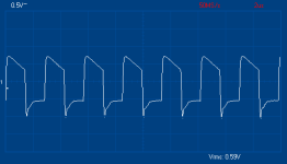
One more thing, the DEM clock signal oscillogram shows significant amplitude jitter, this could indicate a crosstalk or power supply issue.
The DEM clock amplitude should be constant with only very small amplitude fluctuations.
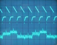
I attached an oscillogram showing the DEM clock, and the active divider output (decoupling capacitor removed), observe the HF noise that needs to be filtered out by these decoupling caps.
The steps are the tolerances between passive dividers that need to be averaged. On the oscillogram two are closely matched, the remaining two are not. Note that BCK (2.8224 MHz) is present at the active divider outputs as well.
The presence of this step signal indicates that the DEM clock is functional, and the TDA1541A internal shift-registers receive a valid DEM clock signal.
One more thing, the DEM clock signal oscillogram shows significant amplitude jitter, this could indicate a crosstalk or power supply issue.
The DEM clock amplitude should be constant with only very small amplitude fluctuations.
I attached an oscillogram showing the DEM clock, and the active divider output (decoupling capacitor removed), observe the HF noise that needs to be filtered out by these decoupling caps.
The steps are the tolerances between passive dividers that need to be averaged. On the oscillogram two are closely matched, the remaining two are not. Note that BCK (2.8224 MHz) is present at the active divider outputs as well.
The presence of this step signal indicates that the DEM clock is functional, and the TDA1541A internal shift-registers receive a valid DEM clock signal.
Attachments
ecdesign,
thank you very much.
I have tested the DC supply at pin 9 of the 74LS161: about 4,6 V. Supply is provided by a TL431 shunt regulator programmed to output 5V, so voltage drop across the series resistor is too high.
I'll also try series resistor at DEM clock output and at spdif receiver output, as you suggest.
Decoupling caps are very small SMD polypropylene 100nF 16V. On pins 13 and 18 the SMD cap is paralleled with a small 1uF 20V polyester cap. All caps are directly soldered under the pins with the shortest possible route to AGND.
What is the best pin to test the active divider output?
Is it worthy to substitutute the 74LS161 with the suggested 74HC161?
I will report after modding.
Best regards.
Paul
I have searched the forum and there is a thread about the TDA1541, I can't recall where I found it. In essence, the +5V, -5V and -15V supply voltages are shared between the digital and analog sections of the chip, i.e. all of the voltages are supplying both the digital and analog part. This is obviously not very good. As I understood the most critical is the -5V that has most influence on the analog output.
Katapum said:Hi all,
I´d like to ask you:
What are the analogue and digitals pins supplies at TDA1541 chip?
Thanks in advance.
Hi Katapum
pse send me your email addres.
I will send you some (Philips) doc's about the TDA1541
It is indeed mixed.
Onno
tubee said:It's mixed. Search for "tda1541 info" here on diy audio
http://www.diyaudio.com/forums/showthread.php?postid=366490#post366490
or
http://www.diyaudio.com/forums/showthread.php?postid=351155#post351155

What´s the truth?
You have PM.Onnosr said:
Hi Katapum
pse send me your email addres.
I will send you some (Philips) doc's about the TDA1541
It is indeed mixed.
Onno
On DEM reclocking again
Hello,
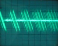
I have now dedicated a single shunt regulator (TL431) to the supply of the 74LS161 (no HC found yet...). But I have found that the amplitude jitter was due to a too low level of the signal injected into pin 16 of the TDA1541A. Previously the signal was tapped from a 680 ohm (at +5V) /330 ohm divider. Now I have substituted the 330 ohm resistor with a 820 ohm one. Now the signal seems OK. Please look at the attached image. Listening response is also positive. Sound is clean as without the DEM reclocking, but with a better focus.
Ecdesign's DEM reclocker is very simple but very effective.
Paul
P.S. The DEM clock has now an amplitude of 1.8 Vpp - 0.6 Vrms. Is this enough to drive the internal oscillator of the TDA1541A?
Hello,
I have now dedicated a single shunt regulator (TL431) to the supply of the 74LS161 (no HC found yet...). But I have found that the amplitude jitter was due to a too low level of the signal injected into pin 16 of the TDA1541A. Previously the signal was tapped from a 680 ohm (at +5V) /330 ohm divider. Now I have substituted the 330 ohm resistor with a 820 ohm one. Now the signal seems OK. Please look at the attached image. Listening response is also positive. Sound is clean as without the DEM reclocking, but with a better focus.
Ecdesign's DEM reclocker is very simple but very effective.
Paul
P.S. The DEM clock has now an amplitude of 1.8 Vpp - 0.6 Vrms. Is this enough to drive the internal oscillator of the TDA1541A?
Attachments
Hi Sandor,
680 / 330 Ohm should provide approx. 1.63 Vpp @ 5V
680 / 820 Ohm should provide approx. 2.73 Vpp @ 5V
If your measurement (1.8 Vpp) is correct, your 74LS164 only outputs approx. 3.3 Vpp, this is the typical "1" output voltage level noted in the 74LS164 datasheet. The 74HC164 should be able to provide output voltages close to VCC.
1.8 Vpp is enough to drive (overrule) the internal DEM clock oscillator. Correct DEM clock operation can be verified by disconnecting one of the active divider decoupling capacitors, and check if there is a step pattern visible that runs in sync with the DEM clock (post #2021).
I have now dedicated a single shunt regulator (TL431) to the supply of the 74LS161 (no HC found yet...). But I have found that the amplitude jitter was due to a too low level of the signal injected into pin 16 of the TDA1541A
680 / 330 Ohm should provide approx. 1.63 Vpp @ 5V
680 / 820 Ohm should provide approx. 2.73 Vpp @ 5V
If your measurement (1.8 Vpp) is correct, your 74LS164 only outputs approx. 3.3 Vpp, this is the typical "1" output voltage level noted in the 74LS164 datasheet. The 74HC164 should be able to provide output voltages close to VCC.
P.S. The DEM clock has now an amplitude of 1.8 Vpp - 0.6 Vrms. Is this enough to drive the internal oscillator of the TDA1541A?
1.8 Vpp is enough to drive (overrule) the internal DEM clock oscillator. Correct DEM clock operation can be verified by disconnecting one of the active divider decoupling capacitors, and check if there is a step pattern visible that runs in sync with the DEM clock (post #2021).
Re: TDA1543 octal D-I DAC schematics

Hi ecdesigns,
While I was copying your schematic in Eagle (yes, I'm gonna build this DAC) I noticed some unconnected wires or wires with wrong names namely (at the left bottom corner of your schematic):
- U23F, pin #13, wire named DI
- U24F, pin#13, wire named WSI
- U24A, pin# 1, wire named BCKI
- U24B, pin# 4, wire named BCK1 (it's low resolution image, so I think it is written BCKone)
My question is where do I connect these wires, are the "I" at the end of DI, WSI and BCKI indicate I2S input ( in my case, I will use I2S direct from SAA7310)?
Also, what I should do with unconnected pins #8 and #9 of U24D, should I left them open or tied to ground?
-ecdesigns- said:
Well I used the OP-amps this way (see added schematic diagram). It's a rough setup for a single board octal D-I DAC using the TDA1543. The timing chain has plenty of taps to build a 16, 32 or 64 D-I DAC using the TDA1543. The setup is balanced / DC coupled since output capacitors are too expensive. Decoupling cap's can be added between each AD823 NON-inverting input (reference) and ground. Enjoy.
Hi ecdesigns,
While I was copying your schematic in Eagle (yes, I'm gonna build this DAC) I noticed some unconnected wires or wires with wrong names namely (at the left bottom corner of your schematic):
- U23F, pin #13, wire named DI
- U24F, pin#13, wire named WSI
- U24A, pin# 1, wire named BCKI
- U24B, pin# 4, wire named BCK1 (it's low resolution image, so I think it is written BCKone)
My question is where do I connect these wires, are the "I" at the end of DI, WSI and BCKI indicate I2S input ( in my case, I will use I2S direct from SAA7310)?
Also, what I should do with unconnected pins #8 and #9 of U24D, should I left them open or tied to ground?
Hi aparatusonitus,
U23F pin # 13, WSI (word select input from source)
U24F pin # 13, DI (data input from source)
U24A pin # 1, BCKI (bit clock input from source)
U24B pin # 4, BCK1 (BCK one) goes to pin #1 of U15 (non-inverted bit clock)
BCKI, WSI, and DI are the I2S inputs
The schematic diagram I posted was only a concept, made a long time ago, a lot has changed since then.
While I was copying your schematic in Eagle (yes, I'm gonna build this DAC) I noticed some unconnected wires or wires with wrong names namely (at the left bottom corner of your schematic):
U23F pin # 13, WSI (word select input from source)
U24F pin # 13, DI (data input from source)
U24A pin # 1, BCKI (bit clock input from source)
U24B pin # 4, BCK1 (BCK one) goes to pin #1 of U15 (non-inverted bit clock)
My question is where do I connect these wires, are the "I" at the end of DI, WSI and BCKI indicate I2S input ( in my case, I will use I2S direct from SAA7310)?
BCKI, WSI, and DI are the I2S inputs
The schematic diagram I posted was only a concept, made a long time ago, a lot has changed since then.
Hi ecdesigns,
Thanks for quick replay...I have one more question for you...U1- U14 at pin #9 have wire named R, where this one goes?
I'm aware of that, but I could not locate a schematic that uses TDA1543 DACs and have DC coupled, balanced output. Any pointers?
Thanks for quick replay...I have one more question for you...U1- U14 at pin #9 have wire named R, where this one goes?
-ecdesigns- said:The schematic diagram I posted was only a concept, made a long time ago, a lot has changed since then.
I'm aware of that, but I could not locate a schematic that uses TDA1543 DACs and have DC coupled, balanced output. Any pointers?
Hi aparatusonitus,
These are the reset inputs, they are connected to VCC.
Thanks for quick replay...I have one more question for you...U1- U14 at pin #9 have wire named R, where this one goes?
These are the reset inputs, they are connected to VCC.
Re: EC, is the DI4T ready for sale?
there's a lot that's not for sale yet I'm guessing that it will all be released "en masse".
MGH said:I don't see it on your website yet. Still working on some bugs?
there's a lot that's not for sale yet
I'm guessing that it will all be released "en masse".Hi ecdesigns,
Thanks for replay and your patience, an digital ignoramus like me just have to ask...even I've found the answer in yours later schematic, just to confirm, that is.
Another question...I've search a bit about Langrangian method of interpolation and found that Wadia holds few patents based on it (namely pat. #5075880, #5226000, #5260704 and #5532950). Wadia use to delay first of four DACs by 1/4th of the frame time, the second DAC is delayed 1/2 of the frame time, the third DAC is delayed 3/4th and the fourth DAc is delayed one full frame time. In your application you chose not to delay first DAC, it's fed directly from I2S lines, do you know any reason why Wadia do that differently?
Hi MGH,
bugs? No, the DI4T prototype performs much better than expected.
The main problem is lack of time. I have a lot of other projects to complete, so the time I can spend on DAC development is limited.
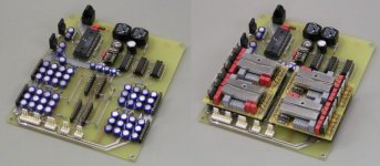
The DI4T uses existing DA1541A, DI8PS, TUBEDIF and TUBEPS modules, some had to be modified slightly. The new modules are the DI4 mainboard, and the optional SPDIF cleaner. I attached some photographs of the new DI4 mainboard.
The mains filters aren't placed on the wrong PCB, they are required for both, passive LC power supply and loop filter.
The local electrolytic capacitor clusters are used to provide peak currents to the DAC modules, preventing long power supply paths.
The complicated timing chain is gone, only two chips are required now. The third chip is for both WS & DEM clock generation. Both phase comparator and pre-scaler chips are mounted underneath the CS8412 socket for shortest possible connections.The 4 UHS clock buffers are mounted on the solder side.
The resistors and wire links, placed on turned pin sockets aren't for experimenting. I put them there to minimize crosstalk.
The low-jitter VCXO master clock is placed on a small PCB. There is no reclocker, the VCXO directly feeds the DAC chips through two UHS clock buffers. The master clock is placed close to the DAC chips, in order to minimize timing jitter.
I still have to add one 5-way connector for the optional SPDIF cleaner module, and partially re-route the PCB for the CS8416.
EC, is the DI4T ready for sale? I don't see it on your website yet. Still working on some bugs?
bugs? No, the DI4T prototype performs much better than expected.
The main problem is lack of time. I have a lot of other projects to complete, so the time I can spend on DAC development is limited.
The DI4T uses existing DA1541A, DI8PS, TUBEDIF and TUBEPS modules, some had to be modified slightly. The new modules are the DI4 mainboard, and the optional SPDIF cleaner. I attached some photographs of the new DI4 mainboard.
The mains filters aren't placed on the wrong PCB, they are required for both, passive LC power supply and loop filter.
The local electrolytic capacitor clusters are used to provide peak currents to the DAC modules, preventing long power supply paths.
The complicated timing chain is gone, only two chips are required now. The third chip is for both WS & DEM clock generation. Both phase comparator and pre-scaler chips are mounted underneath the CS8412 socket for shortest possible connections.The 4 UHS clock buffers are mounted on the solder side.
The resistors and wire links, placed on turned pin sockets aren't for experimenting. I put them there to minimize crosstalk.
The low-jitter VCXO master clock is placed on a small PCB. There is no reclocker, the VCXO directly feeds the DAC chips through two UHS clock buffers. The master clock is placed close to the DAC chips, in order to minimize timing jitter.
I still have to add one 5-way connector for the optional SPDIF cleaner module, and partially re-route the PCB for the CS8416.
Attachments
- Home
- Source & Line
- Digital Line Level
- Building the ultimate NOS DAC using TDA1541A