Hi all,
I'm making a PCM1794A project without the board and cost cutting limitations of the Chinese modules. It's for personal use but I'm wondering if there's demand in which case I could run it as a small commercial venture.
I'm a part-time electronic engineer, more digital than analog but it's easy to do with the datasheets. All digital chips are Texas Instruments apart from the MCU. Here's the spec:
Active power consumption = 5v, 0.67A
Standby power consumption = 5v, 0.02A
I'm using SPDIF but it's becoming difficult to find motherboards with this connection. HDMI requires an extraction chip and introduces jitter, USB introduces complexities for Async mode and most vendors lack specification details. I still concluded for stereo SPDIF is the best source.
I'm also using only a balanced output. I use Adam Audio speakers which in my opinion are the best speakers in the world at a given price point. This however will hinder those without balanced.
Any thoughts, reflections, guidance, much appreciated.
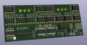
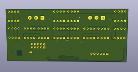
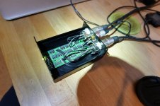
Board pictures are without silk.
I'm making a PCM1794A project without the board and cost cutting limitations of the Chinese modules. It's for personal use but I'm wondering if there's demand in which case I could run it as a small commercial venture.
I'm a part-time electronic engineer, more digital than analog but it's easy to do with the datasheets. All digital chips are Texas Instruments apart from the MCU. Here's the spec:
- 2x balanced outputs, 132db/A
- SPDIF 50PS jitter.
- I2S pins if SPDIF isn't soldered.
- 5v input, can be VBUS and noisy.
- Very low noise LDO's for the 3.3v and 5v audio rails.
- 6x NE5534 or equiv.
- Panasonic 2% film ciltering caps.
- MCU for audio power stage shutdown after 3 minutes.
- Dual 12v/-12v boost & inverter, low ripple.
- LED outputs for power, standby, error, receiving.
- Very small size.
Active power consumption = 5v, 0.67A
Standby power consumption = 5v, 0.02A
I'm using SPDIF but it's becoming difficult to find motherboards with this connection. HDMI requires an extraction chip and introduces jitter, USB introduces complexities for Async mode and most vendors lack specification details. I still concluded for stereo SPDIF is the best source.
I'm also using only a balanced output. I use Adam Audio speakers which in my opinion are the best speakers in the world at a given price point. This however will hinder those without balanced.
Any thoughts, reflections, guidance, much appreciated.
Board pictures are without silk.
Attachments
Lots of itty-bitty SMD. Are you planning to assemble these by hand? Toaster oven solder reflow?
I'm curious which clock/PLL chip you ended up with (the one by the oscillator). Or is that the SPDIF receiver?
I'm also curious about the opening in the ground plane in the corner by the 10-pin connector. What's the idea there?
It looks like a nice and compact module. You might want to add mounting holes. I also appreciate the balanced output. Balanced is the way to go!
Tom
Prototype would be hand assembled, 0603 so easy.
SPDIF is DIR9001.
Unsure which ground plane you're referring to, unless you're referring to the square on the back. That's because there's an inductor on the other side.
No room for mount holes on the current form-factor but I could enlarge it.
Sticker pads are another option.
SPDIF is DIR9001.
Unsure which ground plane you're referring to, unless you're referring to the square on the back. That's because there's an inductor on the other side.
No room for mount holes on the current form-factor but I could enlarge it.
Sticker pads are another option.
I guess there are arguments for and against those cutouts. Some people worry more about eddy currents and reduced inductance, others more about shielding and uninterrupted ground planes. Most switcher evaluation boards I have seen don't make use of cutouts under inductors though.
Any reason for using DIP OpAmps when they are surrounded by 0603 SMDs? Seems like a missed opportunity to implement better parts properly instead of using them on adapters.
Any reason for using DIP OpAmps when they are surrounded by 0603 SMDs? Seems like a missed opportunity to implement better parts properly instead of using them on adapters.
wouldnt it be preferable to optimise the design properly for a particular, high performance modern opamp, rather than limiting it, by allowing for multiple suboptimal parts to be used? the use of sockets and dip8 opamps, lowers performance of the decoupling, lengthens the FB loop of everything and adds paracitics; all so you can 'roll' opamps? you'll be stuck with a generic set of values, so no part will be as well catered for as it would without. basically if you can hear the difference between them, its because something is not working properly.
Last edited:
Quick update.
Board #1 had a few mistakes on it.
Board #2 had too high PP-v on the +/- 12v lines of ~130mV. I redid that power section and switched to four layer. Also fixed op-amp decoupling to be on the same plane. Added mounting holes and switched connectors to JST.
Now running board #3 which I expect will be final. It sounds tremendously good.
My only disappointment is in power consumption. At +/- 12.5v it's consuming VBUS/1A. I thought this was an error at first but in another thread worked out it's normal. I'm now considering given the balanced output is +/- 4.5v that I'll run the +/-12.5v at +/-7.5v. Some consider this bad but there's nothing to suggest in the datasheet it impacts performance as long as there's enough headroom.
Remember you don't need to use symmetric power supplies for the opamps. From what I recall the PCM1794 needs greater negative rail voltage swing on the opamps than positive. So size the positive rail accordingly with the requirements of the summing amplifier on the output.
I seem to recall using +5 -12 on one of my designs where power consumption was important.
I seem to recall using +5 -12 on one of my designs where power consumption was important.
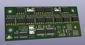
Board #3, final design
As a side question what is the software please that creates this 3D design ? Thank you
Quite correct '5th element', but I don't have a choice as the -12v is generated from the +12v boost supply. The -12v has an additional diode voltage drop but otherwise they're about equal current wise. One behaviour of this approach is one can only get out the same current from the -12v as is being consumed by the +12v line, which is fine for audio op-amps.
Other question - Kicad
Other question - Kicad
Hi all,
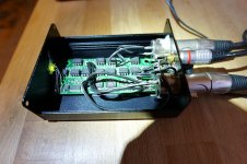
I've now completed this project and will release it.
The program is set to standby after 15 seconds of no audio. It uses < 2mA in standby and about 620mA when active.
It sounds literally perfect. I don't think it gets much better then this.")
I will release the entire project as open-source on my website soon.
I've now completed this project and will release it.
- 4 layer PCB, all gerbers and schematic as kicad project. Zip and upload to jlcpcb for a cheap prototype board.
- MPLABX project for CPU (can be programmed with cheap MPLABX Snap)
- BOM file included, nothing is hard to find
- SMD's are 0603, easy to assemble with reflow station
The program is set to standby after 15 seconds of no audio. It uses < 2mA in standby and about 620mA when active.
It sounds literally perfect. I don't think it gets much better then this.
I will release the entire project as open-source on my website soon.
Attachments
- Home
- Source & Line
- Digital Line Level
- PCM1794A DAC Project