Hi,
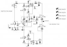
i built this stage iv for the PCM1798 or COD from twisted pear audio, but i don't understand why i have dc offset at the output ( 0.7V) while my j-fets are match paired. I have this problem when I put a cap in C7 and C8.
Someone can help me?
Thank you! Maxpou
i built this stage iv for the PCM1798 or COD from twisted pear audio, but i don't understand why i have dc offset at the output ( 0.7V) while my j-fets are match paired. I have this problem when I put a cap in C7 and C8.
Someone can help me?
Thank you! Maxpou
Attachments
Last edited:
So, when C7 and C8 are removed there is no D.C. offset?
If yes, then measure the D.C. voltage at the drain of Q4 and the gate of Q5, with C7 and C8 in place, to see if they are symmetrical with respect to ground. If there's an imbalance, my first guess is that one of those 1,000uF e-lytic caps may be leaking D.C. Obviously, the offset should not be affected by C7/C8 which should function as open circuits at D.C.
If yes, then measure the D.C. voltage at the drain of Q4 and the gate of Q5, with C7 and C8 in place, to see if they are symmetrical with respect to ground. If there's an imbalance, my first guess is that one of those 1,000uF e-lytic caps may be leaking D.C. Obviously, the offset should not be affected by C7/C8 which should function as open circuits at D.C.
Last edited:

Maybe the FET's are matched but not your resistors (4.7 Ohm). Only a slight mismatch could give this DC offset.
Hi Lampie,
i use the prp resistor 1% and i verified each of them.
Maxpou
Hi Ken,
thank's for reply. my first test was to change the capacitors for 100uF, without success, 2nd I lowered the resistors R8 and R9 by half, without success and my last test was to change my j-fets without success too.
Maxpou
1) Just to confirm, there is no D.C. offset with C7/C8 removed?
2) Also, what are the supply voltage readings at the drain of Q4 and the gate of Q5 with and without C7/C8?
Last edited:
1) Just to confirm, there is no D.C. offset with C7/C8 removed?
2) Also, what are the supply voltage readings at the drain of Q4 and the gate of Q5 with and without C7/C8?
Hi Ken,
no d.c. offset without C7/C8 and i have 10.15V in drain of Q4 and 10.26V in gate of Q5.
Thank's Maxpou
R7 does not have any effect at all?
Hi,
no because i have a coupling cap C2.
Maxpou
Try to put a potmeter of 100 ohm with 10 ohm in series over R6 and check if you can adjust to 0v on the output.
Hi Lampie,
unfortunatly impossible adjust to 0V at output.
Maxpou
Put the 100nF or 47nF close at the JFETs. close or better @ D of Q4 and another decoupling C @ G of Q5.
That is decoupling capacitors all to ground @ gndout point
Leave 1000uF in place, or replace maybe witha a bit smaller value 220uF-470uF?
Hi Zoran,
I had replaced by 100uf and if I put a 0.1uf in parallel with C7/C8 the offset increases to 1.1v.

Maxpou
Disconnect C2 at the point with jfet buffer. Leave 100uF and 100nF C in place.
(This will give You a chance to check IV stage and C. Because of the C not conducting DC should be 0mV at disconnected end. If You have any positive DC C is not good and should be replced.)
Anyway, check the ground connection from input resistor of the jfet buffer stage to central ground, where GND from power supply connected. And solderings too.
Last edited:
What if there is a high frequency oscillation that is throwing off your DVM readings? Wouldn't having capacitors to bypass the resistors help increase the amplitude of the AC output and possibly throw off the DVM even more? Maybe there is an oscillation or other problem or maybe there isn't, but if no scope to check then maybe all you can do are things like take both AC and DC DVM measurements at each node, and maybe see if changing capacitance to ground anywhere in the circuit changes the output offset. In other words, you might be able to get some better idea of what is going on.
What did you find adjusting the resistor value? No change at all?
Another question: Is the output loaded (maybe a small resistor value in series will help (100 Ohm). This will increase the output Z a little but is good practice as it helps protecting the transistors agains short circuit and HF oscillation.
Another question: Is the output loaded (maybe a small resistor value in series will help (100 Ohm). This will increase the output Z a little but is good practice as it helps protecting the transistors agains short circuit and HF oscillation.
Last edited:
Lampie519 has the right sort of idea. Try inserting a 1K resistor in series with the gate of Q4. This will create an RC filter pole in conjunction with the gate terminal's parasitic capacitance, and is known as a 'gate stopper'. Solder the resistor close to the gate terminal of Q4.
Last edited:
- Status
- This old topic is closed. If you want to reopen this topic, contact a moderator using the "Report Post" button.
- Home
- Source & Line
- Digital Line Level
- i/v stage problem