Pics Attached.
“We recommend 40 hours burn-in time...”
Thanks for the pic, all clear, weapons grade BS.
OPINION WARNING:
Wouldn't be concerned about the burn-in thing. I doubt they mean burn-in in an engineering sense. Probably more in an audiophile sense, where it refers to stabilization, or perhaps reaching a state of equilibrium, of subtle 2nd or 3rd order effects that some people can hear on some systems. If you hear them and they bother you then maybe giving the dac some time will make you happier. If you don't hear those things then don't worry about it; doesn't apply.
Wouldn't be concerned about the burn-in thing. I doubt they mean burn-in in an engineering sense. Probably more in an audiophile sense, where it refers to stabilization, or perhaps reaching a state of equilibrium, of subtle 2nd or 3rd order effects that some people can hear on some systems. If you hear them and they bother you then maybe giving the dac some time will make you happier. If you don't hear those things then don't worry about it; doesn't apply.
indeed that eval board is ridiculously priced and bizarro and the schematic barely readable
They put the ultra-expensive *cough* I mean ultra-low-noise, obviously, LDOs on the digital supplies, and some LM317 on the analog supplies. That's an.... interesting... take.
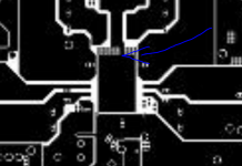
And... there is no ground plane. It's garbage.
The are instructions in the pdf to open the schematic at full resolution. You have to click or double click on it.
Regarding ground planes, ESS says they did tests with separate ground plane segments for analog and digital, but that they found no benefit over a single shared ground plane. Of course, they were measuring with an AP. Maybe it just means any difference didn't show up well on an FFT. A theoretical reason for wanting to try segmented ground plane areas is so that ground current flow paths can more controlled. Some data sheets for recommend controlling ground currents or putting keep outs under some chips. A practice used by some dac designers is to put ground keep outs under the clocks for the same reason (e.g. Topping D90).
Regarding voltage regulators, I use low noise LDOs on clocks and digital circuits, although clocks seem to do best with some little power tweaks. For audio frequency analog circuitry I use different regulators, usually not ultra-low noise LDOs. For very sensitive analog circuitry, I might use a discrete regulator design since there is more control to optimize it for the load. Ultimately, looks to me like Rohm wants the dac to be evaluated by how well people like the sound, not what it took to get there.
Last edited:
 .
.Well considering the layout, I'm not sure it can be further massacred, lol.
I mean the designers of this chip went to the trouble of putting a huge low impedance pad with a "GROUND" label on it, and the intern who made the board connects it to AGND through a tiny 1mm trace lol. And they even went to the trouble of splitting the copper further into AGND, AGNDL, AGNDR, to ensure the maximum noise spot on the board is on top of the DAC. Gotta admire such dedication.
I mean the designers of this chip went to the trouble of putting a huge low impedance pad with a "GROUND" label on it, and the intern who made the board connects it to AGND through a tiny 1mm trace lol. And they even went to the trouble of splitting the copper further into AGND, AGNDL, AGNDR, to ensure the maximum noise spot on the board is on top of the DAC. Gotta admire such dedication.
Attachments
The Pontiff has Spoken!
Just like syn08 to pass judgement without a unit front of him ......") .
.
Maybe we should nickname him Ovidiu Meter Pontiff with all due respect and change his Avatar to something like picture below.
This is all in jest.
Just like syn08 to pass judgement without a unit front of him ......
. Maybe we should nickname him Ovidiu Meter Pontiff with all due respect and change his Avatar to something like picture below.
This is all in jest.
Attachments

Well considering the layout, I'm not sure it can be further massacred, lol.
Markw4 will find a way, wanna bet?
Just like syn08 to pass judgement without a unit front of him ......
Maybe we should nickname him Ovidiu Meter Pontiff with all due respect and change his Avatar to something like picture below.
This is all in jest.
Whoops... Markw4 business associate to the rescue. Perhaps instead of buying useless boards you should invest and buy him a decent oscilloscope.
This is not at all in jest.
Been busy with other stuff, finally got the Rohm eval board powered up just now. It is apparently designed to work with a particular USB board, for which there are mounting holes and an interface header. Happen to have one, so it going to tried first a stock configuration. After, ohhh, say, 40hrs I will probably have more to say.
Well considering the layout, I'm not sure it can be further massacred, lol.
I mean the designers of this chip went to the trouble of putting a huge low impedance pad with a "GROUND" label on it, and the intern who made the board connects it to AGND through a tiny 1mm trace lol. And they even went to the trouble of splitting the copper further into AGND, AGNDL, AGNDR, to ensure the maximum noise spot on the board is on top of the DAC. Gotta admire such dedication.
Don't worry, some people here will claim that ROHM did it on purpose because it "sounds good". Just like the bad practices on the AK4499 EVB.
A theoretical reason for wanting to try segmented ground plane areas is so that ground current flow paths can more controlled. Some data sheets for recommend controlling ground currents or putting keep outs under some chips. A practice used by some dac designers is to put ground keep outs under the clocks for the same reason (e.g. Topping D90).
This only demonstrates a total lack of understanding on the part of those doing what you have described.
They put the ultra-expensive *cough* I mean ultra-low-noise, obviously, LDOs on the digital supplies, and some LM317 on the analog supplies. That's an.... interesting... take.
And... there is no ground plane. It's garbage.
Yes, the grounding on it is convoluted and not much help for those wanting to apply the chip. it seems to be built for tweakers, with the through-hole resistors and places for opamp rolling.
Well considering the layout, I'm not sure it can be further massacred, lol.
I mean the designers of this chip went to the trouble of putting a huge low impedance pad with a "GROUND" label on it, and the intern who made the board connects it to AGND through a tiny 1mm trace lol. And they even went to the trouble of splitting the copper further into AGND, AGNDL, AGNDR, to ensure the maximum noise spot on the board is on top of the DAC. Gotta admire such dedication.
You've met Mark, right?
I hadnt spotted the grounding faux pa in my cursory look, once I saw one layer was blurred, I clicked away. thats ridiculous there is no GND plane. its one thing to use minimal slots and guards in a single plane to control return current, it's another entirely to chop it up into little pieces without providing a solid plane at all. I can just imagine the spray of RF from all that. It goes totally against best practices. I had assumed the silly priced regs (with expensive bypass caps at the reg, rather than at the load), were on the AVCC, your conclusion of *** backwards digital vs analogue regs is hilarious. They clearly spent a lot of time on the layout, but didnt do the basics right.
This only demonstrates a total lack of understanding on the part of those doing what you have described.
yes, to see ESS, AKM AND ROHM all stuck in last century design; chopping it all up into tiny pieces is frustrating; you look to application notes and EVM to get the best out of your parts. increasing impedance of ground and supply, while simultaneously increasing the bandwidth of the parts and forgetting that RF will find a way that isnt what you planned? ... le sigh.
Last edited:
They clearly spent a lot of time on the layout, but didnt do the basics right.
They also spent a time to describe in DS the power-on and power_off sequence, but I didn't saw any sequence in their EVB schematic - all regulators have enable on..
- Home
- Source & Line
- Digital Line Level
- Luxman uses ROHM Semiconductor MUS-IC BD34301EKV dac