Since the latch signal is crucial to get the best performance from a DAC we are developing a FIFO re-clocker that runs slave to the master clock.
In other words the FIFO buffer and re-clocker FPGA based does not manage the latch of the DAC (WS signal in I2S format and LLLR in PCM format) that comes directly from the master clock via a programmable divider isolated from the other digital circuits.
This to avoid any interference between the FPGA based digital circuit and the conversion circuit inside the DAC.
Every time the latch signal switches new data are asked to the FPGA, using all optical isolated lines.
This is a different approach in respect to other similar devices where the FPGA works on all I2S signals including the word select.
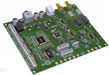
There will be 3 boards, the main FIFO re-clocker and the optional User Interface and Output Interface boards.
The main board has 4 I2S input selectable by the User Interface board.
Also the dithering process is selectable via the User Interface board.
There are 2 output options, both with header and u.fl connectors.
The main board needs 2 master clock signals, one for each sample rate family.
It can accommodate the Crystek or NDK oscillators, but a pair of very low phase noise are strongly suggested (5.6448 MHz up to 24.576 MHz).
More infos next days, a prototype is on the way.
New RPI Interface, LVDS transmitter and receiver I2S over HDMI from post #125
The Well synchronized asynchronous FIFO buffer - Slaved I2S reclocker
User manuals at post #153
The Well synchronized asynchronous FIFO buffer - Slaved I2S reclocker
In other words the FIFO buffer and re-clocker FPGA based does not manage the latch of the DAC (WS signal in I2S format and LLLR in PCM format) that comes directly from the master clock via a programmable divider isolated from the other digital circuits.
This to avoid any interference between the FPGA based digital circuit and the conversion circuit inside the DAC.
Every time the latch signal switches new data are asked to the FPGA, using all optical isolated lines.
This is a different approach in respect to other similar devices where the FPGA works on all I2S signals including the word select.
There will be 3 boards, the main FIFO re-clocker and the optional User Interface and Output Interface boards.
The main board has 4 I2S input selectable by the User Interface board.
Also the dithering process is selectable via the User Interface board.
There are 2 output options, both with header and u.fl connectors.
The main board needs 2 master clock signals, one for each sample rate family.
It can accommodate the Crystek or NDK oscillators, but a pair of very low phase noise are strongly suggested (5.6448 MHz up to 24.576 MHz).
More infos next days, a prototype is on the way.
New RPI Interface, LVDS transmitter and receiver I2S over HDMI from post #125
The Well synchronized asynchronous FIFO buffer - Slaved I2S reclocker
User manuals at post #153
The Well synchronized asynchronous FIFO buffer - Slaved I2S reclocker
Attachments
Last edited:
There are several output types available: I2S fixed length (32 bit), I2S variable length (selectable data length) and PCM.
The output formats available are: Two's complement, Offset binary (TDA1541A) and a custom format (sign magnitude + first 3 MSBs thermometer decoded) to be used with our new discrete DAC.
The data length is selectable from 16 up to 32 bit.
The bit clock mode is selectable between stopped clock adn continuous clock.
It accepts sample rate from 44.1 up to 384kHz.
The FPGA digital circuit is totally isolated from the master clock section using high speed optocouplers.
The master clock selection between the two sample rate families is performed using relè instead of digital multiplexer.
We have took the maximum care to avoid any RF interference between the FPGA section and the clock section.
The master clock section uses a separate power supply (3V3), we suggest battery power supply. We are developing a LiFePo4 power supply system, it will be available next months.
Andrea,
I don't like digital multiplexer, too. However, the relay can be problematic due to impedance mismatch and coil interference. BTW, it is possible to reclock critical signal (i.e. LE, BCK) with independent flip-flops? I'm afraid octal flip-flops tend to interfere with each other inside the package.
I don't like digital multiplexer, too. However, the relay can be problematic due to impedance mismatch and coil interference. BTW, it is possible to reclock critical signal (i.e. LE, BCK) with independent flip-flops? I'm afraid octal flip-flops tend to interfere with each other inside the package.
Andrea,
I don't like digital multiplexer, too. However, the relay can be problematic due to impedance mismatch and coil interference. BTW, it is possible to reclock critical signal (i.e. LE, BCK) with independent flip-flops? I'm afraid octal flip-flops tend to interfere with each other inside the package.
There is no coil interference since double coils latching relays have been used. LE
Is reclocked at output with master clock. BCK is not a crucial signal and so it is optically isolated from the master oscillators and not reclocked.
Andrea,
Is it similar to Iancanada FIFO reclock? Or it will better performance?
What is the min. divider, can it use 6 MHz clock for 96 or 192KHz sample rate?
Thanks, and good job!
192 khz pcm and 96 khz i2s
I see some regulators on board. Will you consider better ones like LT3045? Or, just add an external power connector.
LDO on board are just to power FPGA and MCU, so there is no reason to use better ones. Only for master clock and divider a very good power supply is needed, battery suggested.
")
woud you please explain - will this device contribute sync clocking between source and dac
There are 2 time domains, so this device works in asynchronous mode. The incoming I2S data are stored in a memory buffer, then there are a pair of external oscillators that provide the master clock. Via a programmable divider the master clock is divided down to get the Latch Enable to feed directly the DAC (the latch signal does not cross the FPGA. The output data from the FPGA are synchronized to the LE, in other words at the rising edge of the latch enable the FPGA provides a new word of data. There is no interaction between Fpga/Mcu and master clock/dividers section (that are optically isolated). There is an optional board to optically isolate bit clock and data coming out from the FPGA and the DAC input.
There are 2 time domains, so this device works in asynchronous mode. The incoming I2S data are stored in a memory buffer, then there are a pair of external oscillators that provide the master clock. Via a programmable divider the master clock is divided down to get the Latch Enable to feed directly the DAC (the latch signal does not cross the FPGA. The output data from the FPGA are synchronized to the LE, in other words at the rising edge of the latch enable the FPGA provides a new word of data. There is no interaction between Fpga/Mcu and master clock/dividers section (that are optically isolated). There is an optional board to optically isolate bit clock and data coming out from the FPGA and the DAC input.
Andrea, the DDDAC group is using the FiFoPi to re-clock the signal for the DAC with good succes, specially when your clock is involved. I saw this topic, which looks like a FiFoPi, with the different perspective, that you claim that the word clock is the most important and is the only signal being reclocked (?) This might be the case with the PCM63, but not for the PCM1794. I just wanted to state that here before anyone thinks this re-clocker can be used with a DDDAC.
Unless I missed the point and it is not only the LR clock being re-clocked?
May be you can elaborate on the difference with the FiFoPi?
thanks!
Doede
oh by the way, in the PCM1794, ultimately the SCK is the most critical. The SCK determines when the oversampled output updates, so reducing jitter on that line would reduce discrepancies on the output
- Home
- Source & Line
- Digital Line Level
- The Well synchronized asynchronous FIFO buffer - Slaved I2S reclocker