I've attached a PDF version of the current revision, REV -1, of the schematic. It has quite a bit of the parts from the evaluation board manual in, now I need to add the DIR chip, add a bunch more jumpers, add power supplies, and make sure that the nets in my drawing match up with the nets in the eval board manual. That will bring us up to REV 0. Next steps from there are going to be adding the inputs I need, removing a lot of
"unnecessary" dip switches to move towards full software control, adding a microcontroller to do serial control of the 3 chips. Hopefully at this point I will lay out all the different modular subboards. After that will come focusing more on the clocks and output stage, the ability to swap both of those should be quite useful.AK_DAC.pdf - Google Drive
"unnecessary" dip switches to move towards full software control, adding a microcontroller to do serial control of the 3 chips. Hopefully at this point I will lay out all the different modular subboards. After that will come focusing more on the clocks and output stage, the ability to swap both of those should be quite useful.AK_DAC.pdf - Google Drive
Regarding support for DAC pin control mode, it is not usable for playing DSD and unnecessary if an MCU is available. Simply poking 0x8F into register address 0x00 will cause it to auto play any PCM audio sent from I2SoverUSB. Arduino code for that is trivial and is something I could provide in the form a simple app to read and write any I2C register address. That could eliminate the need for lots of switches and wiring, but its up to the designer.
AK4137 is a little more complicated in that not all functions are controllable using either pin-mode or serial-mode. There needs to be some mix of the two. Not hard to wire it up so that any pins can be controlled from an 8-bit I2C addressable latch logic chip.
AK4137 is a little more complicated in that not all functions are controllable using either pin-mode or serial-mode. There needs to be some mix of the two. Not hard to wire it up so that any pins can be controlled from an 8-bit I2C addressable latch logic chip.
Last edited:
Regarding the schematic, there are some errors in the eval board manual schematic verses the as-built dac chip daughterboard. Mostly it has to do with silkscreen labels, but probably wise to check what you have against pictures I posted of the top and bottom of the daughterboard.
Looks like some little SMD Schottky diodes are missing adjacent to the dac on your schematic, although they are shown in the eval board manual schematic for the daughterboard.
It may help to know that someone else started on another AK4499 project then unexpectedly had to stop. It was for a different end use than your project, but you might find some schematics there to cross check with. https://www.diyaudio.com/forums/dig...-ak4499eq-adc-dac-boards-116.html#post5908519 (link to post #1152 in that thread)
Last edited:
Regarding support for DAC pin control mode, it is not usable for playing DSD and unnecessary if an MCU is available. Simply poking 0x8F into register address 0x00 will cause it to auto play any PCM audio sent from I2SoverUSB. Arduino code for that is trivial and is something I could provide in the form a simple app to read and write any I2C register address. That could eliminate the need for lots of switches and wiring, but its up to the designer.
AK4137 is a little more complicated in that not all functions are controllable using either pin-mode or serial-mode. There needs to be some mix of the two. Not hard to wire it up so that any pins can be controlled from an 8-bit I2C addressable latch logic chip.
Do you have any info on AK4137's DPLL bandwidth or behavior, or filter responses?
I ask because one day I might get to work on a personal project again and I want to like this chip, but AKM gives you nothing in the datasheet compared to AD, TI, and Cirrus. I know the devil that is the SRC4392. If you compare the headline specs that AKM is touting, the CS8421 looks better than the SRC4x92... but in reality the SRC4x92 can be better if you are using it with a jittery source.
Now, I would guess all these chips are audibly transparent, but I hate rewarding bad documentation.
To me, I would like to use AK4137 because it has 1.8V logic level support.
Last edited:
Adam, looking your schematic again it looks like I/V opamps may be planned to be located somewhat distant from the dac chip. The I/V opamps need to be located close by because their feedback loops pass through the dac chip to be closed. The example set by the eval board design is good since it keeps the physical loop areas of the I/V opamp feedback loops reasonably small.
Last edited:
Somoloko,
The output pins with the same signal names are supposed to be paralleled as has been done by Adam.
Chris,
Don't know about AK4137 jitter rejection nor other unpublished information for it. I suggest to use it only because the eval board does and because it has the interesting ability to convert PCM to DSD256.
Last edited:
Hi Adam,
I have taken a look at your ak4499 schematic and saw you are missing values for zener diodes in jung style regulators. Those can be found in AK4495SEQ EVB documentation. BTW I am going to use a more usual looking jung regulator with "proper filtering" of reference (will use spx2431 - low noise version of TL431).
Cheers, Kovax
Yes, I know there are still many parts missing and definitely some errors. I will try and address a couple of the points mentioned here:
MarkW4, though the Op-amp feedback loop may seem large in the schematic, I plan on keeping it short in the physical assembly. I'm going to try and convey this better in the schematic though. I'm thinking of doing a board stack, maybe using samtec board to board connectors to keep the feedback loops as short as I can. I'd really rather avoid doing them on the same board, because I would like to be able to switch the I/V stage independently of the DAC. In terms of different modules that I would like to have / be able to swap, I would like to have each regulator be on a daughterboard, or maybe blocks of identical regulators / regulators for a specific domain. I would then like to split up each of the 3 AKM chips into their own board, have a daughterboard for the microcontroller, one for the clock circuitry, one for USB input, and a backplane board. There are going to be many different boards, in stacks of various heights on the backplane.
MarkW4, though the Op-amp feedback loop may seem large in the schematic, I plan on keeping it short in the physical assembly. I'm going to try and convey this better in the schematic though. I'm thinking of doing a board stack, maybe using samtec board to board connectors to keep the feedback loops as short as I can. I'd really rather avoid doing them on the same board, because I would like to be able to switch the I/V stage independently of the DAC. In terms of different modules that I would like to have / be able to swap, I would like to have each regulator be on a daughterboard, or maybe blocks of identical regulators / regulators for a specific domain. I would then like to split up each of the 3 AKM chips into their own board, have a daughterboard for the microcontroller, one for the clock circuitry, one for USB input, and a backplane board. There are going to be many different boards, in stacks of various heights on the backplane.
Making what might be more or less a 'Buffalo' or 'Acko' AK4499 dac seems like a questionable idea to me. It may be what people think they want though. Some psychology research shows that people think they would like many options, but when faced with too many they tend to make poor decisions. Most people are actually happier with only a few options once they get whatever it was they were shopping for.
Also, there is really no need for optional I/V stages, IMHO. It may be someone could develop a possibly better I/V, but opamp swapping is not likely to be helpful. Its not a weak point with the dac now. Respectfully suggest to not encourage people to do things are are likely to make the dac worse (things some Audiophiles mistakenly do, a subject too long to go into for this post).
All the foregoing IMHO only, of course.
Yes, you make a good point, at this stage however I would like to keep the design as modular and open as possible, I have some ideas on how to keep the FB loop shorter than the Buffalo Style. I'm also not building this for commercial purposes yet, would just like a dac experiementation test bed that can be shared and iterated upon openly by the community.
where that came from
Somoloko,
The output pins with the same signal names are supposed to be paralleled as has been done by Adam.
where that came from
The AK4499 data sheet lists all the pins, for example one entry in the table says:
Pins____Name________Discription
83,84__ IOUTL2P__O__ Current Output pin (L2ch positive signal).
The column with a capital O in it indicates the signal is an output.
In other words, the exact same signal is on two pins, probably in order to help keep output impedance very low.
Also, the schematics for the AK4499 eval board show the pins connected in parallel.
Nothing is lost by doing that since from the description you can see they are both the same signal: Left-side, Channel-2, Positive output (positive phase, if you want to use that term). There are another two pins for the negative signal (or negative phase). No information is lost. Each unique output signal passes through its own I/V stage then goes all the way to the differential output XLR connector for that channel.
Hopefully that makes sense. If not, please let us know.
+1+1
I agree wholeheartedly with Marks input to this thread with respect to power supplies based on my experience with many different regulator types on other DACs. It would be nice if more respect could be shown to people who are just trying to get the best outcomes.
John
Do you have any info on AK4137's DPLL bandwidth or behavior, or filter responses?
Chris, I contacted AKM about this ages ago and the support engineer was not
able to come up with any info.
Same with ComTrue ASRC (forget the part no).
T
Made some changes to the I/V stages so that they hopefully more resemble the schematic, however I find the schematic provided in the evaluation manual essentially unusable. It's been a lot of effort to get it into something more readable from the mess of wires they give you. The old link should still be good, here it is again:
AK_DAC.pdf - Google Drive
AK_DAC.pdf - Google Drive
Adam,
Probably no need for 4-wire control. Basically, its a version of SCI bus.
I2C bus should be fine for everything, IMHO.
Differences basically are that SCI can run much faster, but it has a Select line for each device on the bus which can add up to a lot of select lines.
I2C is slower (although fast enough for us) and is device addressable so that only two wires and ground can be shared by several devices.
")
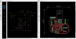
have started doing pcb from latest pdf attached few posts up.. but must confess i have not fully understand this vref part of circuit, especialy opamp inputs part. maybe better i continue tomorow, here is preview. please advise if you see something that needs change, gnd vias and other details will put later.
Attachments
Last edited:
- Home
- Source & Line
- Digital Line Level
- AK4499 DAC Design