During my development of TDA1387-based DACs I came to the tentative conclusion that fewer chips was generally better in SQ terms. That was based on experience that strongly hinted that the power supply was the limiting factor and that more chips meant heavier demands on the supply. I also found that more output current made an I/V stage (other than a purely passive one) harder to get sounding good.
The power supply sensitivity turned out to be in large degree dependent on the variation in output voltage at the DAC's current outputs - purely passive I/V usually has the largest output voltage variation, consequently the highest sensitivity to power supply rail noise. By 'noise' here I don't just mean random noise, normally load-induced (i.e. signal correlated) noise is a bigger influencer of SQ.
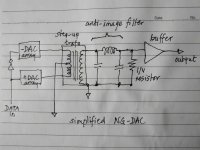
A 'lightbulb' moment came when I considered that a step-up transformer could be used to ensure a very low voltage variation at the DAC's output whilst still allowing a high enough I/V resistor to be used so as not to need a voltage gain stage to create a 2VRMS output signal. Use of a step-up transformer isn't new, Audio Note had a patent on it (now expired). What is new is using a high ratio step-up transformer in conjunction with a very large number of paralleled DAC chips - the parallel array allows an even smaller variation of DAC output voltage and hence lower power supply sensitivity.
I've attached an outline sketch of the arrangement. A large number of paralleled DACs generates a peak current in the region of a few tens of mA. The DAC arrays are arranged to generate that current in 'push-pull' mode (aka 'balanced') so that there isn't any need to block the DC through the trafo - the DC currents are applied out of phase and hence cancel within the core of the trafo. The secondary of the trafo has typically 100X the turns of the primary meaning the standard 2VRMS is generated directly from 20mV at the DAC and only needs filtering (to attenuate images) and buffering to create a low output impedance for driving cables and a power- or pre- amp.
From my earliest experiments with a step-up transformer, I found that the primary inductance is what creates the LF roll-off and that the usual core material I use (PC40) doesn't give enough inductance (or have high enough mu in other words) to give an optimized design. So I have moved over to using 10K material which has about 4X higher mu but a lower peak flux capability. There aren't too many forms of core that this 10K material turns up in (at least in off-the-shelf quantities) on Taobao, I have for my earliest public design settled on using EP17. The wish to create a fully balanced design means using two EP17s per channel, for a total of 4. Fortunately they're cheap to buy on Taobao, the main cost is going to be in the labour to wind them.
Gerbers are attached for a 36 DAC board - four of these are needed to feed into the 4 EP17 transformers so that the output created is 2VRMS across the I/V resistors. In the sketch the output filter's shown single-ended but for the first design I'm going balanced, necessitating doubling up on filter and buffers, leading to a transformer between the two phases for creating a single-ended output.
The power supply sensitivity turned out to be in large degree dependent on the variation in output voltage at the DAC's current outputs - purely passive I/V usually has the largest output voltage variation, consequently the highest sensitivity to power supply rail noise. By 'noise' here I don't just mean random noise, normally load-induced (i.e. signal correlated) noise is a bigger influencer of SQ.
A 'lightbulb' moment came when I considered that a step-up transformer could be used to ensure a very low voltage variation at the DAC's output whilst still allowing a high enough I/V resistor to be used so as not to need a voltage gain stage to create a 2VRMS output signal. Use of a step-up transformer isn't new, Audio Note had a patent on it (now expired). What is new is using a high ratio step-up transformer in conjunction with a very large number of paralleled DAC chips - the parallel array allows an even smaller variation of DAC output voltage and hence lower power supply sensitivity.
I've attached an outline sketch of the arrangement. A large number of paralleled DACs generates a peak current in the region of a few tens of mA. The DAC arrays are arranged to generate that current in 'push-pull' mode (aka 'balanced') so that there isn't any need to block the DC through the trafo - the DC currents are applied out of phase and hence cancel within the core of the trafo. The secondary of the trafo has typically 100X the turns of the primary meaning the standard 2VRMS is generated directly from 20mV at the DAC and only needs filtering (to attenuate images) and buffering to create a low output impedance for driving cables and a power- or pre- amp.
From my earliest experiments with a step-up transformer, I found that the primary inductance is what creates the LF roll-off and that the usual core material I use (PC40) doesn't give enough inductance (or have high enough mu in other words) to give an optimized design. So I have moved over to using 10K material which has about 4X higher mu but a lower peak flux capability. There aren't too many forms of core that this 10K material turns up in (at least in off-the-shelf quantities) on Taobao, I have for my earliest public design settled on using EP17. The wish to create a fully balanced design means using two EP17s per channel, for a total of 4. Fortunately they're cheap to buy on Taobao, the main cost is going to be in the labour to wind them.
Gerbers are attached for a 36 DAC board - four of these are needed to feed into the 4 EP17 transformers so that the output created is 2VRMS across the I/V resistors. In the sketch the output filter's shown single-ended but for the first design I'm going balanced, necessitating doubling up on filter and buffers, leading to a transformer between the two phases for creating a single-ended output.
Attachments
Last edited:
Lower complexity design - Q-gross DAC
Since soldering up four DAC boards and interconnecting them is really only for the true hair-shirt brigade of multibit die-hards (myself very definitely included) I was wondering if it would be possible to design a 'gateway DAC' based on this model but which called for far fewer DAC chips. Turns out, it is and I have the first prototype playing into my ears as I type. This will eventually allow a DAC to be built using just two PCBs - as soon as the PCB layout for the analog board gets done, anyway")
The lower number of DAC chips comes at a price as there are no free lunches and its paid in terms of the output compliance voltage at the DAC chips. The trafo of the Q-gross (quarter-gross) DAC has only a 1:25 step up ratio so ~40mVRMS exists at those pins, whereas on the 4 PCB design, that's down to ~10mVRMS as the transformer gives 100X voltage gain. The analog PCB is agnostic towards the number of DAC chips used, the difference will just be in the winding details of the EP17 trafos used. In theory its possible to accommodate even more than 144 TDA1387s although I've yet to figure out a way of fitting the thicker wire on the transformer's bobbin. There has to be some way though.....
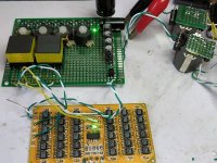
In the photo, the analog board containing CLC filters, trafos and buffers is at the rear - it feeds into RM10 cores (rear right) wound as output bal-SE trafos. The DACs themselves are fed from a TL431 shunt at 4V and the whole is powered from a single 6V rail.
Since soldering up four DAC boards and interconnecting them is really only for the true hair-shirt brigade of multibit die-hards (myself very definitely included) I was wondering if it would be possible to design a 'gateway DAC' based on this model but which called for far fewer DAC chips. Turns out, it is and I have the first prototype playing into my ears as I type. This will eventually allow a DAC to be built using just two PCBs - as soon as the PCB layout for the analog board gets done, anyway
The lower number of DAC chips comes at a price as there are no free lunches and its paid in terms of the output compliance voltage at the DAC chips. The trafo of the Q-gross (quarter-gross) DAC has only a 1:25 step up ratio so ~40mVRMS exists at those pins, whereas on the 4 PCB design, that's down to ~10mVRMS as the transformer gives 100X voltage gain. The analog PCB is agnostic towards the number of DAC chips used, the difference will just be in the winding details of the EP17 trafos used. In theory its possible to accommodate even more than 144 TDA1387s although I've yet to figure out a way of fitting the thicker wire on the transformer's bobbin. There has to be some way though.....
In the photo, the analog board containing CLC filters, trafos and buffers is at the rear - it feeds into RM10 cores (rear right) wound as output bal-SE trafos. The DACs themselves are fed from a TL431 shunt at 4V and the whole is powered from a single 6V rail.
Attachments
Since soldering up four DAC boards and interconnecting them is really only for the true hair-shirt brigade of multibit die-hards (myself very definitely included)...
I admire your tenacity but doesn't there come a point where the sensible thing would be to make the investment in a reflow oven based soldering regime?
Where are you getting all the TDA chips?
As I set out on the lingDAC thread, I'm not sure that a reflow approach would in fact be more efficient in time. Partly because I prefer to test the DACs first, with only power applied and partly because these chips are already desoldered and they're not mechanically consistent from part to part as fresh parts off the reel would be. They have excess solder on many pins and on the sides of the package which sometimes leads to shorts between pins. The pins are also bent out of shape in many cases so they're not all in contact with the PCB which makes me wonder if they'll be amenable to reflow.
The chips are from Taobao.
The chips are from Taobao.
From my earliest experiments with a step-up transformer, I found that the primary inductance is what creates the LF roll-off
This would be resolved if the i/v resistor is on the primary side of the transformer and loads the dacs outputs directly, right?
No, not according to my simulations in LTSpice - the LF roll-off was the same. But the LF gain gets reduced by the ratio between the I/V resistor's value and the DCR of the primary which was something of a surprise, given I'm still a greenhand in working with trafos. Meaning a primary with significantly lower R than the I/V resistor is needed to transmit all the output current of the DACs to the secondary.
Hi Richard,
Have you tried transformer I/V after the current mirror? I'm currently applying a 10k:10k transformer after OPA861. It has DCR around 2k, so I don't need the I/V resistor. Due to the limited swing voltage of OPA861, I have to trim the output voltage by paralleling a resistor on the primary side. The trafo also takes care of the LPF, so minimum parts are used here.
Poting
Poting - no, I'm not using any kind of active circuitry in current mode. Simply a buffer (an EF biassed by a CCS) fed from the I/V resistor. Entirely passive prior to the I/V. In my experience a trafo as LPF is a bit hit-and-miss in that the leakage inductance (which provides the series element of an LC filter) is difficult to predict and has rather large variation.
No, not according to my simulations in LTSpice - the LF roll-off was the same.
How do you represent the DAC output? A voltage source in series with a resistor? How big a resistor?
As I set out on the lingDAC thread, I'm not sure that a reflow approach would in fact be more efficient in time. Partly because I prefer to test the DACs first, with only power applied and partly because these chips are already desoldered and they're not mechanically consistent from part to part as fresh parts off the reel would be. They have excess solder on many pins and on the sides of the package which sometimes leads to shorts between pins. The pins are also bent out of shape in many cases so they're not all in contact with the PCB which makes me wonder if they'll be amenable to reflow.
Ah, OK. Fair enough. I didn't clock that properly before. I guess it would also ask questions about the resilience of the chips to repeated heating.
I had a look at the gerbers in a viewer - the PCBs are smaller than I imagined!
AoE 3rd mentions a current input topology named a "regulated cascode", which finds use in high-bandwidth photodiode transimpedance amplifiers (up to dozens or hundreds of MHz). In this one, input voltage noise is determined by one transistor while current noise is determined by the other. Seeing your thread, maybe this would be something of use for an I/V? Transformers, while undeniably useful, are notoriously messy.
Thanks for the suggestion - in the case of active I/V I nowadays always like to have a filter between it and the DAC's output. This rather constrains I/V circuits in that they need to have a well-defined, constant input impedance (vs frequency and vs amplitude) and the lower, the better. Putting a trafo into the circuit was my solution to the conundrum of the DAC wanting a low load impedance and the I/V circuit wanting to be relatively higher input impedance.
I set out some background thinking here : How a transformer helps... | Details | Hackaday.io
I set out some background thinking here : How a transformer helps... | Details | Hackaday.io
In theory its possible to accommodate even more than 144 TDA1387s although I've yet to figure out a way of fitting the thicker wire on the transformer's bobbin. There has to be some way though.....
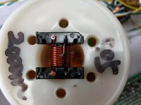
I came up with a way to get fewer turns on the transformer - add the CT later with thinner wire. Here I have 6+6 T for the primary (0.62mm) and there's enough room left for 4000T of wire for the secondary (0.05mm). This gives an impedance ratio of ~111k meaning an 11k I/V resistor on the secondary represents 0.1ohm to the DAC array. Initial listening indicates a slight improvement in LF - the price is the need for a lot more DAC chips - at least 128.
Attachments
New set of DAC board gerbers on the way
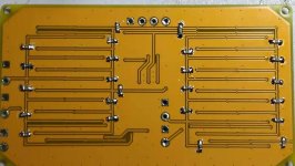
From building up stacks of the DAC boards I found there was some very low-level hiss when listening at low digital volumes (its masked at higher volume settings). I eventually tracked this hiss down to less than perfect grounding - the groundfill is a bit too contorted to give a low enough impedance for the DACs. The remedy on the existing PCBs is to attach some 0603 0ohm links as straps to give lower ground impedance. Picture attached - I've used a couple of dozen 0 ohm links (one is 0805, all others 0603) soldered where the soldermask is scratched away with a craft knife.
A new set of PCBs with the grounding fixed will be along within a week, but if you're going to build a DAC with the gerbers I've already published you'll want to consider adding some 0 ohm straps. I didn't notice any hissing effects on a single PCB, it became apparent on a stack of 3 and gets worse with more boards added beyond that.
Attachments
Last edited:
Thanks @abraxalito, looks like this project is reaching final stage. What I2S device would you recommend? I see your post here: USB->HDMI->SPDIF a waste of time?
However I would prefer modern low jitter device with asynchronous USB transfer like this one with XU-208, three premium oscilators and CPLD chip, see the post by @obscurus. He tested it working with PhiDAC, it seems compatible. If you order one for testing, it will be on my account and risk. I need at least three. If stops working, it doesn't affect payment. lingDAC - cost effective RBCD multibit DAC design
EDIT: It doesn't say about availability of drivers. This one has the same PID/VID as Amanero device: WEILIANG AUDIO Combo384 USB to I2S digital interface refer to Amanero 384kHz/32bit DSD512|amanero usb|usb to i2s|breeze audio - AliExpress - 11.11_Double 11_Singles Day
However I would prefer modern low jitter device with asynchronous USB transfer like this one with XU-208, three premium oscilators and CPLD chip, see the post by @obscurus. He tested it working with PhiDAC, it seems compatible. If you order one for testing, it will be on my account and risk. I need at least three. If stops working, it doesn't affect payment.
lingDAC - cost effective RBCD multibit DAC designEDIT: It doesn't say about availability of drivers. This one has the same PID/VID as Amanero device: WEILIANG AUDIO Combo384 USB to I2S digital interface refer to Amanero 384kHz/32bit DSD512|amanero usb|usb to i2s|breeze audio - AliExpress - 11.11_Double 11_Singles Day
Last edited:
EDIT: It doesn't say about availability of drivers. This one has the same PID/VID as Amanero device...
IIRC, the Chinese Amanero clones work with Amanero Windows drivers, but the firmware is an old version that doesn't support ASIO or DSD. Trying to burn newer Amanero firmware will brick it. Thus, it is no better or worse than the Chinese XMOS boards. Also despite what the picture shows, many of those boards are now shipping with black plastic non-crystal clock oscillator modules. Such clocks have more jitter than appropriately selected crystal clocks.
The best USB board I have tried (out of several, including some with plug-in clock modules) is JLSounds I2SoverUSB. Sorry, it does cost more than a Chinese clone. However, it can be transferred to a new dac and used for multiple dac projects over a long period of time. Jitter is very low and it is configurable for various dac chips: I2SoverUSB - I2S over USB Audio
http://jlsounds.com/uploads/I2SoverUSB v.III.pdf
Last edited:
The best USB board I have tried (out of several, including some with plug-in clock modules) is JLSounds I2SoverUSB. Sorry, it does cost more than a Chinese clone. However, it can be transferred to a new dac and used for multiple dac projects over a long period of time. Jitter is very low and it is configurable for various dac chips: I2SoverUSB - I2S over USB Audio
http://jlsounds.com/uploads/I2SoverUSB v.III.pdf
I second that recommendation. The JLSounds board, which I use, have proven to be excellent and completely reliable. IMO they're superior to the Amanero (especially the version 3 which matches the Amanero data rates) because they have onboard isolation and reclocking. Their other stuff is good too.
I wouldn't use a Chinese Amanero clone - too many bad tales about them, apart from which they represent IPR theft.
Last edited:
Also despite what the picture shows, many of those boards are now shipping with black plastic non-crystal clock oscillator modules. Such clocks have more jitter than appropriately selected crystal clocks.
I believe these are XOs from SiTime, like SiT8208 series.
Thanks @abraxalito, looks like this project is reaching final stage. What I2S device would you recommend? I see your post here: USB->HDMI->SPDIF a waste of time?
At this stage I don't have any particular recommendations to make - the guy in that link wanted an interface for his Nexus tablet and I have experience getting Android phones working with those simple, cheap first generation USB chips.
The I2S (and S/PDIF) source I use from my PC is based on CMedia CM6631A. Its async but has an annoying feature that after the PC has hibernated, the S/PDIF output stops working and it needs to be power cycled to function again.
CM6631A???? USB?I2S/SPDIF?????32/24Bit 192K??DAC-???
(Note this one is an updated model, mine is a bit long in the tooth now).
- Home
- Source & Line
- Digital Line Level
- Grossly parallel multibit DAC adventures