Progress update
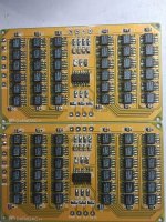
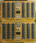
Four boards with the new layout have been now listened to and don't suffer from the low-level hiss the old layout does, which is good news. I was going to release the gerbers for that but in the meantime we decided to try out another experiment - using thicker copper to get a lower impedance, both to the supply rail and to the output pins of the DACs. When paralleling a large number of (over 100) chips the effective impedance the transformer presents is going below 100mohm hence the resistance of the tracks to the chips starts to become significant. A minor change was made to the layout for this 2oz copper experiment - the output pads are now more conveniently placed to connect twisted pairs to.
In other news the PCB layout of the main analog board has begun. For this board the aim is to have almost all through-hole components - just the NP0 capacitors for the LC filters will be SMT - that hopefully makes building a kit less daunting for those whose eyes or dexterity (or both!) is/are challenged. The buffers (see my sketch in first post) are being built out of SMT parts as there are just too many components to fit within the 10*10cm window (for a cheap PCB) if the resistors for those cannot be SMT. The buffers are going to be plug-in modules so anyone who shies away from SOT-23 package soldering can order them ready-made. Having modules also means others can experiment with their own designs for the buffers.
Attachments
Just listened to the four boards in a stack which were built with the latest layout and 2oz copper. One chip was found to be broken amongst the 144 on those boards. Tracking a dud chip down isn't too difficult so long as the failure of the chip is such that the pin7 multiplying effect isn't also broken (which so far I haven't found). The faulty DAC normally gives its presence away when digital volume is set very low (below -50dB) and sounds like static breakthrough modulated by the music at a level which is louder than the music itself. Shorting each DAC's pin7 to 0V in turn eventually reveals which chip contributes the hash.
Since this new layout is now good to go, I've attached the gerbers and also the schematic. The RC network values on the schematic diagram are just place holders for now and depend on the characteristics of the transformers which are attached - the higher the step-up ratio, the lower the Rs and higher the Cs.
Since this new layout is now good to go, I've attached the gerbers and also the schematic. The RC network values on the schematic diagram are just place holders for now and depend on the characteristics of the transformers which are attached - the higher the step-up ratio, the lower the Rs and higher the Cs.
Attachments
That's pretty cool! Did you ever happen to try different numbers of DAC chips to find the optimum? I suspect it's a matter of diminishing returns at some point, if true, it would be nice to find the optimal point.
With all these DAC chips, you have a good amount of current available. What are your thoughts on passive I/V with so many DACs in parallel? Or other, simpler I/V solutions, such as a basic op-amp?
Need pics of the final product!")
With all these DAC chips, you have a good amount of current available. What are your thoughts on passive I/V with so many DACs in parallel? Or other, simpler I/V solutions, such as a basic op-amp?
Need pics of the final product!
Hi Matt - thanks for joining in here! I can't say (so far) that there really is an optimum, I've built various DACs up over the past few months with chip counts ranging from 36 (single board) up to 288 (eight board stack) and the subjective differences have been pretty subtle. The measurable change when going to higher chip counts is the variation of voltage on the DAC output pins goes down - i.e. with more chips the I/V stage input impedance goes down, and faster than the increase in output current from the DACs.
Passive I/V (direct into a resistor) with so much current available certainly works though I can't really see the point unless a very low output impedance is the only target. There must be some noise cancellation going on in such a situation though I would guess the advantage of such is undone by the increased sensitivity to PSU noise from having so many paralleled chips. I'd not recommend using many paralleled DACs into an opamp for I/V - the opamp's classAB output stage's modulation of the PSU rails would be the likely bottleneck subjectively.
Pics will certainly come in due course - today I'm going to be checking the first draft layout of the analog board then I can put up an interim pic of what that's going to look like.
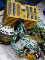
Here's a pic to whet your appetites - those of you who yearn for DAC chip counts into 3 figures that is. This is a stack of 8 PCBs - the original layout PCBs - so the total number of chips is 288. I built the stack as an experiment to see how low a supply voltage a TDA1387 could tolerate and still deliver untarnished audio. Turns out, around 2V or about 1V below its datasheet minimum. (That can't be useful with passive I/V though as there's no output compliance to speak of then.) Lots of chips in parallel are needed when running such low supplies as the output current scales with supply voltage. Hence the 8 board stack. The advantage of lower supply voltage is much lower operating power - power scales as (supply voltage)^2.
Attachments
So ... why y'all be a sugar daddy and send a couple o' FREE samples this here way.Here's a pic to whet your appetites - those of you who yearn for DAC chip counts into 3 figures that is. .
For those who yearn for freebies, it was said from the beginning - no frieebies - beggars may go away.
@abraxalito. Did you test a single board with 96/196kHz sample rate? Do it make sense to populate every second DAC chip and double number of boards for such application? I think of using empty space for extra decoupling.
I do consider new boards as a great progress. Good work.
@abraxalito. Did you test a single board with 96/196kHz sample rate? Do it make sense to populate every second DAC chip and double number of boards for such application? I think of using empty space for extra decoupling.
I do consider new boards as a great progress. Good work.
So far no, I haven't tested at 96k or 192k, just at 88k2. A little higher current draw compared to 44k1. I will have a play at higher rates just to see what happens though. Why do you want extra decoupling incidentally? You can slap extra ceramics across the top of the chips if you're so inclined but I can't see the benefit.
I've increased the height of the board stack from 8 to 10 boards now, for a grand total of 360 chips. Its working fine, sounding awesome at just 2.1V. I had a supercap board lying around so I've connected that to the supply, it has 61 * 10F EDLCs on it. Didn't notice any improvement in sound when I brought it in so I figure heroics on the supply is only of marginal benefit. But can't hurt for extra bragging rights as supercaps have a certain 'cachet'
I've increased the height of the board stack from 8 to 10 boards now, for a grand total of 360 chips. Its working fine, sounding awesome at just 2.1V. I had a supercap board lying around so I've connected that to the supply, it has 61 * 10F EDLCs on it. Didn't notice any improvement in sound when I brought it in so I figure heroics on the supply is only of marginal benefit. But can't hurt for extra bragging rights as supercaps have a certain 'cachet'
For those who yearn for freebies, it was said from the beginning - no frieebies - beggars may go away.
@abraxalito. Did you test a single board with 96/196kHz sample rate? Do it make sense to populate every second DAC chip and double number of boards for such application? I think of using empty space for extra decoupling.
I do consider new boards as a great progress. Good work.
@abraxalito. Did you test a single board with 96/196kHz sample rate? Do it make sense to populate every second DAC chip and double number of boards for such application? I think of using empty space for extra decoupling.
I do consider new boards as a great progress. Good work.
Actually I was thinking about larger film or electrolyte caps, one per two (or four) DAC chips, depends how it will fit. It is more effective in removing medium and high frequency components when placed close to the chip than a one large battery of supercaps on the PSU.So far no, I haven't tested at 96k or 192k, just at 88k2. A little higher current draw compared to 44k1. I will have a play at higher rates just to see what happens though. Why do you want extra decoupling incidentally? You can slap extra ceramics across the top of the chips if you're so inclined but I can't see the benefit.
96k sample rate support is important for decoding 48kHz (or 96kHz material), so please do... While I do belong to those who claim that getting higher is not beneficial for SQ, it looks like that 24-bit audio data stream come on the expense of a higher clock rate, our clock chip must keep going. If 16/192kHz works fine, then 24/96kHz should work as well. Padding irrelevant information is wasting of bandwith, but in some cases we have no control.
As for lowering Vcc even further, I didn't even think about, this is shocking, maybe I am thinking to conservative.
BTW, I walked out immediately after posting and now can't delete dupe, sorry.
Last edited:
I ran a very quick test - 96k worked fine at 2.1V but 192k was hissy. So I upped the supply to 2.5V and tried again - success @192k. I would guess that 192k was running at 32bits per sample (since that's what my AK4113 S/PDIF input chip spits out) - presumably 384k/16bits would also work fine at 2.5V.
Oh, absolutely no problemo....BTW, I walked out immediately after posting and now can't delete dupe, sorry.
'Bout them FREE samples ... I saw no mention of "no freebies" anywhere.
BTW: I give fair reviews.
I've been at the "Y" for almost prodigious 13 years ... and am one of the most-respected members of the DIY community.
Experimental filter
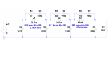
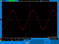
In the world of NOS DACs, unfiltered (or very lightly, first-order filtered) outputs seems to be the norm. However with my engineering background unfiltered hasn't sat well with my instincts and I've often wondered if NOS wouldn't get even better with closer-to-textbook filtering. I used a 5th order filter for lingDAC, PhiDAC has a 3rd order filter as does the first prototype of this 'GrossDAC'. When I looked on my 'scope at the output with a sine stimulus though, even with lingDAC's two-inductor filter, the higher frequencies appear rather messy. There aren't any 'stair-steps' visible of course but there is apparent modulation by image frequencies.
In order to get a visibly clean output on a 'scope, it seems a 7th order filter is required. Here's an example filter and output - I even figured out how to get a screendump from my 'scope (its menu is all in Chinese).
Attachments
screenDUMP
Anyway, the screenDUMP looks great ... congrats on figurin' that out and postin' it.
"Clean"??? How do you get that outta somethin' with a "Gross" in its title?In order to get a visibly clean output on a 'scope, it seems a 7th order filter is required. Here's an example filter and output - I even figured out how to get a screendump from my 'scope (its menu is all in Chinese).
Anyway, the screenDUMP looks great ... congrats on figurin' that out and postin' it.
I second that recommendation. The JLSounds board, which I use, have proven to be excellent and completely reliable. IMO they're superior to the Amanero (especially the version 3 which matches the Amanero data rates) because they have onboard isolation and reclocking. Their other stuff is good too.
I wouldn't use a Chinese Amanero clone - too many bad tales about them, apart from which they represent IPR theft.
Imho, I do agree. Abrax is too muchminimizing the importance of this stage and his great design may stay a collosus with clay feet. A pity because his good ideas about outputt stages.
Then he should also consider isolation on usb as we stay bellow 24/96 and go also with bufering-reclocking. And q further ground isolation before the reclocking. We are all aware jitter is less important for those old multidacs however improvments stay great enough... night and day....
While his phrpose is maybe to stay cheap, that's the only way to know if the job around the dac chip worths it. Scope at the outputt will not say all, ears are stupborns....
Last edited:
Hi @diyiggy - I don't understand how I'm minimizing the importance of the input stage as my DAC designs so far haven't included it, they're I2S only. Could you explain?
I've not yet noticed any significant differences from the various input stages I've tried so far (SD card player, AK4113, CM6631A, PCM2706) - that doesn't mean the differences don't exist just that so far I've not trained myself to notice them. In my design process I focus on minimizing aberrations that I do hear in general, but I do from time to time make stabs in the dark out of pure curiosity just to see how something I imagine will sound.
I've not yet noticed any significant differences from the various input stages I've tried so far (SD card player, AK4113, CM6631A, PCM2706) - that doesn't mean the differences don't exist just that so far I've not trained myself to notice them. In my design process I focus on minimizing aberrations that I do hear in general, but I do from time to time make stabs in the dark out of pure curiosity just to see how something I imagine will sound.
Hi Abrax,
Of course I may be wrong, I stayed on the idea your last design has an I2S inputt stage with a gnd vias and a pcm2706 chip feeded itself with the laptop usb outputt ?
Could you describe your streaming chain till the dac pcb please ? My point is you don't hear it becquse you didn't try more recent design a la iancanada for instance.
You talk about sd card, do you not hear a difference vs a noiser solution as streaming from a laptop ?
For my limited experience and only in the redbook area, the way you inputt the I2S is 30 to 50% of improvment on the sound.... I m mostly listen to tda 1541a dac chip but worked on the others till they stop to produce dac chips...
Of course I may be wrong, I stayed on the idea your last design has an I2S inputt stage with a gnd vias and a pcm2706 chip feeded itself with the laptop usb outputt ?
None of my designs have been published with a PCM2706 USB interface. I have used that chip in some example complete DACs - I even got a PCB made with it on - but no schematics nor PCBs have been released publicly.
Could you describe your streaming chain till the dac pcb please ? My point is you don't hear it becquse you didn't try more recent design a la iancanada for instance.
I don't listen to music via streaming in general. Mostly I use my PC (running Foobar) feeding a CM6631 interface (USB->S/PDIF) then a transformer isolated AK4113 from S/PDIF->I2S. I sometimes use a Taobao SD card player (I2S out) based on an STM32F407 chip. I've not tried any of IanCanada's designs you're right.
You talk about sd card, do you not hear a difference vs a noiser solution as streaming from a laptop ?
I don't use a laptop. When I use a PC as a digital source I'm aware its noisy which is why I use a transformer on my S/PDIF receiver. In fact the CM6631 card also has a transformer so I'm double insulated from PC noise.
For my limited experience and only in the redbook area, the way you inputt the I2S is 30 to 50% of improvment on the sound.... I m mostly listen to tda 1541a dac chip but worked on the others till they stop to produce dac chips...
Our experiences differ - I've not found the way the I2S is input making a difference unless the source of that I2S is noisy. There are ways of mitigating that noise - using a transformer is one such, arranging the grounding so that CM noise bypasses sensitive circuits is another. Best use both of these methods together (belt and braces) as CM noise is insidious. If you look at the grounding on the PhiDAC PCB you'll see I use star grounding on the I2S input - this mitigates CM noise. Have you checked how IanCanada protects his DACs against CM noise on the digital input?
While I am personally interested in various digital input options for a GrossDAC, all recent designs by the @abraxalito (LingDAC, through PhiDAC SE) assume I2S input without going into details how it is implemented. I think as a right approach to leave it as an option to the user, as there are number of DIY projects and commercial modules on the market we can chose.
There is no reason to discuss in this thread which I2S interface module (with reclocking, isolation, whatever) is better other than pointing out that such option do exist.
There is no reason to discuss in this thread which I2S interface module (with reclocking, isolation, whatever) is better other than pointing out that such option do exist.
Last edited:
- Home
- Source & Line
- Digital Line Level
- Grossly parallel multibit DAC adventures