The inductors L1-L8 are shown as pairs on the schematic:
Do I need 2 windings in parallel on the P14 cores, or just a single winding?
You only need one winding. The reason for two inductors is because the PCB gives two options - either ready-made Mouser-sourced inductors or DIY ones using the P14 cores.
And am I correct that the target inductance is 27mH total between the pins?
I believe so, I will check back against my old schematics.
Is the mentioned 6+6t : ~4000t generally right for the EP17 input transformers on a halfGross? This would be CT primary and CT secondary.
No, half-gross means only 72 chips and hence needs quite a few more turns on the primary. If my memory is correct it was around 15+15t, I need to look back.
And I have the output RM10s as single primary, CT secondary 1:2?
That's right so as to give the option of SE or balanced output.
Good luck with winding and do take care not to give yourself RSI like I did!
No, half-gross means only 72 chips and hence needs quite a few more turns on the primary. If my memory is correct it was around 15+15t, I need to look back.
I've consulted my notebook from 2020 and found that for the Q-gross I went with 5400 turns of 0.04mm on the secondary, 250 turns of 0.16mm on the primary. So to build a H-gross you'll increase the turns ratio. This means in practice 126 turns on the primary. All windings CT'd.
If you're going for 4000 turns on the secondary then the primary will reduce in proportion, to 94 turns.
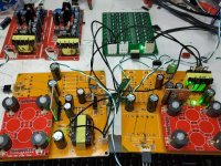
2nd generation GrossDAC
The last few days I've been working on improving the original GrossDAC design - there's a new DAC board where individual shunt regs are used per pair of DAC chips. And on the I/V filter board I'm experimenting with an off-the-shelf transformer.
In this first prototype the output transformer isn't needed as its feeding my monoAMPs which come already equipped with input trafos. The filter boards are 5th order but I'm using up some prototype 9th order boards which for some obscure reason I have too many of.
The eagle-eyed may notice a small green prototype board in the middle - this comes with two IR LEDs to provide a mid-point bias for the centre tapped trafos. I'm running the DAC offset current through the transformer at the moment which may turn out not to be optimum.
Attachments
Last edited:
The 2nd generation prototype sounded acceptably good but thinking a bit more about lowering the noise I wondered if using a cascode MOSFET rather than the input trafos wouldn't be a lot simpler. I'd been playing with a MOSFET in a similar position in my experiments with enhancing the original PhiDAC design. In that instance it was primarily to provide level shifting, but on GrossDAC it can provide impedance transformation with level shifting as a bonus.
I am keeping the 1k resistors for termination of the filter as I'm way too lazy to redesign the filter and wind another set of inductors for it. This though means with the raw output current from the DAC board of 18mA p-p that the swing into the resistor becomes rather large - 18V p-p. But its acceptable as I have an output transformer to bring the voltage down again. In fact I just have to increase the step-down ratio into my amps from ~6 to ~36. The LM317 needs re-configuring to give a 24V supply and the reference (for mid-rail) goes up to 13V. The buffers needed their bias reducing so as not to overheat.
(more to come)
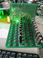
Here's the 2nd prototype DAC board for the design that has the place holder name 'DenaDAC'. The hand-wired interface PCB at the back holds 8 current sources (4 up, 4 down) and 4 MOSFETs to cascode the DAC outputs and give the potential for a big voltage swing.
I found an old pair of EE35 transformers which I'd originally wound as input trafos for GrossDAC, they're now being used as output transformers with 40:1 step down ratio. Which turned out to give the right drive to a TDA8932.
The resulting SQ is the best I've ever heard from TDA1387, completely addictive.
Attachments
PCB revision
The updated 36 DAC board (with cascode FETs included) is being built. This one uses multiple paralleled FETs to spread the load (since the FETs are those tiny SOT-23s) then in theory I should be able to go above the 18V output swing I achieved on the earlier prototype. Whether that'll result in a gain in SQ is what this experiment is all about")
Can't usefully go any higher than 36 chips on a single board as we've reached the maximum cheap board size with this one (10*10cm). Still the capability exists to wire a couple of these in parallel.... I'm not at present planning going beyond 36V swing as I don't have thin enough wire for the primary of the trafo for that so an extra board allows the I/V resistor to scale down in value.
The updated 36 DAC board (with cascode FETs included) is being built. This one uses multiple paralleled FETs to spread the load (since the FETs are those tiny SOT-23s) then in theory I should be able to go above the 18V output swing I achieved on the earlier prototype. Whether that'll result in a gain in SQ is what this experiment is all about
Can't usefully go any higher than 36 chips on a single board as we've reached the maximum cheap board size with this one (10*10cm). Still the capability exists to wire a couple of these in parallel.... I'm not at present planning going beyond 36V swing as I don't have thin enough wire for the primary of the trafo for that so an extra board allows the I/V resistor to scale down in value.
Attachments
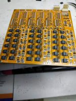
Its been rather a while since I last posted but progress in getting the 'Stack DAC' playing engrossing music has encouraged me along the path of exploring more paralleled chips and led me back to giving this board another shot. I had shelved it due to MOSFETs continually oscillating and/or blowing up but now I figure I probably just had a dodgy reel of FETs. So I'm replacing the 2N7002s with Toshiba SSM3K335s and going to give it another try. Plus I plan to 'overclock' the DAC chips with the pull-up resistor to pin7 to eke out a little more juice...
I apologize beforehand if I seem impertinent in posing this question. I examined the provided schematic for the DenaDac TDA1387 boards, and I noticed that you do not have any passive part connected to pin 7 of the TDA1387. I am accustomed to seeing other designs with a capacitor from pin 7 to ground. Even the datasheet provides for a 1uF cap connected to pin 7 to ground. Will your scheme work without a cap to pin 7 ? Has the DenaDac v2 with the gerbers provided functioning? If it is functional, would you care to explain why pin 7 has been left unconnected?Just listened to the four boards in a stack which were built with the latest layout and 2oz copper. One chip was found to be broken amongst the 144 on those boards. Tracking a dud chip down isn't too difficult so long as the failure of the chip is such that the pin7 multiplying effect isn't also broken (which so far I haven't found). The faulty DAC normally gives its presence away when digital volume is set very low (below -50dB) and sounds like static breakthrough modulated by the music at a level which is louder than the music itself. Shorting each DAC's pin7 to 0V in turn eventually reveals which chip contributes the hash.
Since this new layout is now good to go, I've attached the gerbers and also the schematic. The RC network values on the schematic diagram are just place holders for now and depend on the characteristics of the transformers which are attached - the higher the step-up ratio, the lower the Rs and higher the Cs.
You are quite correct that there's no pin7 cap. We did a listen between having pin7 connected (using a 1210 PPS 1uF cap) and having nothing on pin7. I noticed no difference and my wife even very slightly preferred no cap over a 1uF on pin7. Hence no cap is fitted.
- Home
- Source & Line
- Digital Line Level
- Grossly parallel multibit DAC adventures