You introduce more conversion (linearity) error without RTZ on a pulse by pulse basis then you do by the extra edge transitions (as there should be) with correct RTZ conversion.
Thnx! In general I look at this error as data correlated noise (and distortion), enhancing the edge speed (20 pS) and not having such big voltage swings also helps the time edges need, hence the sonic non-rtz winner here.
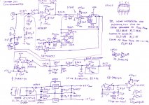
I'm building a 4-Flip Flop dac, which can be made to work as an stereo interleaved dac element, a 4 channel dac or a stereo dual fir. Front end is not ready yet to accomodate all of this, but at least this part is ready to go to the pcb manufacturer soon and there'll be room to experiment to check all this.
Your last picture shows 4 volt bulk caps, any particular reason to go for a 3v3 supply when you can go for 5 or even 6 volts?
Soldering techniques looking aok to me, great work and excellent measurement results indeed, very nice to see this!
Your last picture shows 4 volt bulk caps, any particular reason to go for a 3v3 supply when you can go for 5 or even 6 volts?
Caps where only mounted for photo
") , the array on this design operates at 4.5V as the design is USB powered and we struggle with the 500mA USB current limit, although we will still be a little over......
, the array on this design operates at 4.5V as the design is USB powered and we struggle with the 500mA USB current limit, although we will still be a little over......The larger Array design operates at upto 6V1...
Soldering techniques looking aok to me, great work and excellent measurement results indeed, very nice to see this!
Thank you, however:-
If you look closely you can see damage to the solder resist + uneven size of solder on each pad, but the results of the "Quick" test was that I can work with such small packages... Although I do worry about the larger array as its not easy to QC each solder joint (as they are under the package) and the larger array has many more packages... We have an PCB XRay machine in the lab, but its not something you want to use for each PCB - the array covers a large and its not easy to QC each individual PCB joint...
I'm just programming the P&P machine so I hope better results from machine built boards.... I REALLY hope...!
Measurement where from a larger array design (8 element), the simple two element array design PCB I'm currently building will have lower performance - I expect a DNR of somewhere between 118dB to 124dB and a FS THD of say 110dB...
A 124dB dynamic range would be great as it would match the results of our designs using ES9038Q in Dual diff (limited by the noise of the analogue output stage used on our budget designs).
Keen for the results ASAP
Last edited:
Any DAC array design will become more sensitive to Master Clock Phase noise with more edge transitions (increased clock rate) by 20LogN with N being the clock rate increase, ie 6dB more sensitive to MCLK Phase noise with a doubling of clock frequency.
We use FIR analogue filtering on the DAC array WITH RTZ encoding (well atleast on the larger array designs) - with ANY pulse DAC design if you dont normalises the energy contribution of each "pulse" you will incur THD+N, its unavoidable due to the error of finite edge times - the ONLY method I'm aware to remove the error introduced by real world applications is to implement RTZ.
Thank you very much for your detailed information.
Are A7AJ and N9AB a high-speed logic gate with galvanic isolation? Then high OSR(512 or 1024) DSM pulse train with FIR analog filtering is fed to the analog stage. What I still can't understand is coexistence with FIR analog filter, which is probably the same meaning as analog FIR that I use for my no DAC.Analog FIR in my project means the sum of 1bitDSM pulse train with one clock delay. The attached pic is 42taps analog FIR in 4th order DSM(128OSR). It has vertical 28 resolutions; amplitude usage is 28/42=67%. High order(8th) is usually around 50%. The more, the better if you want excellent SNR. 4th order is theoretically superior to 8th as long as out of band noise is ignored.
I have tried several times to use RTZ encoding but failed to have good results. High OSR and the digital process of RTZ aren't difficult, where much advantage exists because they are in the digital domain. As long as I know, RTZ goes back to zero before the next pulse to ensure the same pulse energy. The very problem is all tap becomes zero before the next pulse. The center position of the attached pic is 21 if the coding is NRZ; the sum of 21 ones and 21zeros results in 21. If you use RTZ in 3 to 1(3/4 is one, 1/4 is zero), 3/4 period is 21; it's the same as NRZ. But 1/4 period is 0 because all tap is zero. The lowest position of the pic is 7(21-14=7). 0 means you can't have an analog-like sine wave like the pic, which means distortion. That's why I can't employ RTZ. I guess I have a fatal misunderstanding. But I couldn't find the answer yet why RTZ can coexist with analog FIR. Please correct me if I'm wrong.
Attachments
Thank you for your feedback. I have understood RTZ in 1 to 1(1/2 is one, 1/2 is zero) with half-cycle delay can get rid of the gap. But I guess RTZ in 1 to 1 has less amplitude usability, which means less SNR. I don't know RTZ can outperform NRZ in numbers. Anyway, I need to learn more about RTZ. Thanks.
You can get rid of the gaps when you make the pulses 0 for half the clock period, apply half-cycle delays between taps (for example by alternating rising and falling edge clocking) and make sure that there are always two taps with the same weight.
Wouldn't that be totally depending on the duty cycle, inverting clock = inverting the duty cycle = changing the timing of the addition of the alternating energy packets?
Indeed, but in the most usual implementations the widths of the pulses depend in the same way on the duty cycle as the delays. In fact this is why you need pairs of taps with (nominally) equal weights, so that random variations of the duty cycle will not (or hardly) affect the sum.
For example, with eight taps:
clock high: output signal = weighted sum of taps 1, 3, 5 and 7, the rest is made zero
clock low: output signal = weighted sum of taps 2, 4, 6 and 8, the rest is made zero
When taps 1 and 2 have equal weights and the same holds for 3 and 4, for 5 and 6, for 7 and 8, and the shifting arrangements are made properly, the exact position of the falling edge within each clock cycle ideally doesn't affect the output signal.
(In practice random duty cycle variations will still modulate the position of the switching spike between the odd and the even taps, but that has much less impact than random duty cycle variations have in a single RTZ DAC.)
Thank you very much for your detailed information.
Analog FIR in my project means the sum of 1bitDSM pulse train with one clock delay. The attached pic is 42taps analog FIR in 4th order DSM(128OSR). It has vertical 28 resolutions; amplitude usage is 28/42=67%. High order(8th) is usually around 50%. The more, the better if you want excellent SNR. 4th order is theoretically superior to 8th as long as out of band noise is ignored.
I have tried several times to use RTZ encoding but failed to have good results. High OSR and the digital process of RTZ aren't difficult, where much advantage exists because they are in the digital domain. As long as I know, RTZ goes back to zero before the next pulse to ensure the same pulse energy. The very problem is all tap becomes zero before the next pulse. The center position of the attached pic is 21 if the coding is NRZ; the sum of 21 ones and 21zeros results in 21. If you use RTZ in 3 to 1(3/4 is one, 1/4 is zero), 3/4 period is 21; it's the same as NRZ. But 1/4 period is 0 because all tap is zero. The lowest position of the pic is 7(21-14=7). 0 means you can't have an analog-like sine wave like the pic, which means distortion. That's why I can't employ RTZ. I guess I have a fatal misunderstanding. But I couldn't find the answer yet why RTZ can coexist with analog FIR. Please correct me if I'm wrong.
I look at RTZ as a amplitude shift. There's just less amplitude (and less low frequency modulation).
So you're saying that because with RTZ there's many times that the FIR runs empty (all zero's)?
But per same time (integrated) it's the same time duration of zero's, right?
Also, at first glance you'd expect RTZ to be able to go to higher modulation depth than, let's say 67% (less lower frequency modulations because of the alternating 1's at low rates, less ISI), but as you said: the zero's are constantly full on.
I'm guessing that this is one of the reasons why John advocates for differential signals, I'd like to know if there needs to be carefull matching of these differential signals (or if distortion levels at high modulation depth go down when matched better).
The main drawback of RTZ is the need for a higher bitclock. For jitter this seems to be great because of the faster edges of the XO, for low phase noise not so.
Would like to know how all of you correlate/solve those higher phase noise clocks vs jitter?
Indeed, but in the most usual implementations the widths of the pulses depend in the same way on the duty cycle as the delays. In fact this is why you need pairs of taps with (nominally) equal weights, so that random variations of the duty cycle will not (or hardly) affect the sum.
For example, with eight taps:
clock high: output signal = weighted sum of taps 1, 3, 5 and 7, the rest is made zero
clock low: output signal = weighted sum of taps 2, 4, 6 and 8, the rest is made zero
When taps 1 and 2 have equal weights and the same holds for 3 and 4, for 5 and 6, for 7 and 8, and the shifting arrangements are made properly, the exact position of the falling edge within each clock cycle ideally doesn't affect the output signal.
(In practice random duty cycle variations will still modulate the position of the switching spike between the odd and the even taps, but that has much less impact than random duty cycle variations have in a single RTZ DAC.)
I wholeheartedly agree, but now it's getting almost philosophical: the idea once was to let go of having to match power supply levels, resistors, temperatures etc and let every piece of silicon add to the signal. DSD does just that. Once you divide it into sectors (odd and even) and have to weigh those later you're almost back to square one.
Of course, it's not as bad as a good ol' thermometer DAC, and this is a good solution to the problem, but I also see it as a step back.
Choices choices. So many of them, right?!
Has anybody ever tried to use a clock signal and pass it to the output when data signal = 1 and otherwise not? It would just mean to have a good switch, or a logic AND. There'll always be a 0 after it etc.
Btw aren't you describing the interleaved dac? I read it has much less hf noise, but don't know why.
Have a good weekend you all!
I look at RTZ as a amplitude shift. There's just less amplitude (and less low frequency modulation).
So you're saying that because with RTZ there's many times that the FIR runs empty (all zero's)?
But per same time (integrated) it's the same time duration of zero's, right?
Also, at first glance you'd expect RTZ to be able to go to higher modulation depth than, let's say 67% (less lower frequency modulations because of the alternating 1's at low rates, less ISI), but as you said: the zero's are constantly full on.
The modulation depth of DSM depends on the order. The best is the 1st or 2nd order DSM, which can have almost 100%. As long as I have experienced, 3rd is 75%, 4th is 65%, 5th is 55%, and more than 6th is 50%. Less modulation depth means less SNR because the signal can't be large while noise is the same level. The maximum amplitude of DSM is usually smaller than PCM by 6dB(50%) because of high order DSM(more than 6th). RTZ has another burden because of the inherent zero. If RTZ is 1 to 1(50% duty cycle), a half is always zero, which results in another 6dB loss; total signal loss is 12dB(if more than 6th order). So, I want to use at least RTZ with3 to 1(2.5dB loss instead of 6dB), but the gap caused by inherent zero isn't avoidable unless you use RTZ with 1 to 1(6dB loss).
I don't know if RTZ can outperform NRZ or not. I have been an NRZ person in my DSM career. That's why I will play with NRZ for the time being. I'm sure the correct IO pad assignment of FPGA is promising. If I could find a way that has additional improvement on SNR by 1dB, my goal(120dB SNR) is truly achievable with NRZ.
I wholeheartedly agree, but now it's getting almost philosophical: the idea once was to let go of having to match power supply levels, resistors, temperatures etc and let every piece of silicon add to the signal. DSD does just that. Once you divide it into sectors (odd and even) and have to weigh those later you're almost back to square one.
Of course, it's not as bad as a good ol' thermometer DAC, and this is a good solution to the problem, but I also see it as a step back.
Choices choices. So many of them, right?!
Has anybody ever tried to use a clock signal and pass it to the output when data signal = 1 and otherwise not? It would just mean to have a good switch, or a logic AND. There'll always be a 0 after it etc.
Btw aren't you describing the interleaved dac? I read it has much less hf noise, but don't know why.
Have a good weekend you all!
I don't know what you mean by the interleaved dac, so I don't know if I'm describing it. It could very well be that I am.
I have made single RTZ circuits a few times when I didn't care too much about the dynamic range, see for example
Simple second-order sigma-delta for checking raw DSD interfaces
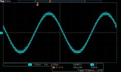
Running a similar circuit at 28.224 MHz, see the attachment, I got dynamic range figures of 88.2 dB(A), or 83.2 dB unweighted up to 20 kHz. The layout was about as bad as it gets: perfboard with wires and no ground plane. The distortion was around -63.55 dB measured with music (Shabba Ranks: House mouse) rather than sine waves. Mind you, the dynamic range values are probably a bit optimistic because I used a DAC running on the same clock as the ADC, which cancels out the effects of close-in phase noise and slow duty cycle fluctuations.
In some other thread JohnW commented that he prefers using a clock-synchronous circuit at some much higher clock frequency over the flip-flop and NOR circuit I use, because my circuit relies on the delay of the flip-flop being long enough. That is, it definitely has to be longer than the mismatch in delays between the NOR gate inputs and preferably long enough for the NOR gate, excluding its internal output buffers, to settle completely. (This applies to a unit RTZ DAC, no matter whether it is or isn't part of a FIRDAC.)
Getting back to RTZ FIRDACs with half-cycle delays, suppose you made such a circuit with an exceptionally poor batch of resistors: so bad that only one tap makes contact, all others are open. You then have a simple single RTZ DAC after all. As soon as the resistors are better than this, you get some of the performance gains that FIRDACs can provide. For example, when all odd tap resistors are 5 % too high and all even tap resistors 5 % too low, you should already get 20 dB less sensitive to random duty cycle fluctuations (assuming that the impact of switching spike phase modulation doesn't dominate). With +/-1 % that's already 34 dB.
Attachments
Last edited:
No DAC... You are trying to build a DAC.
//
yes, a No DAC DAC
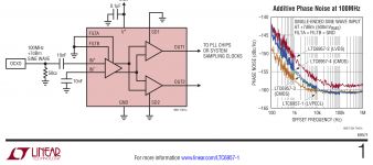
I've repeated many times, but 5V CMOS AC logic has LOWEST phase noise of all logic families I've tested - lower then ECL, and far lower the LVDS...
Dropbox - Logic Phase Noise.jpg - Simplify your life
We use ECL where speed is required above say 200MHz, but suffer the higher phase noise...
Repetition does not make that true. The graph you keep publishing is in
Crawford's Synthesizer Design Handbook from 20 years ago, with credit given
to a microwave trade magazine from another 15 years ago. Both Crawford (whom I
like generally) and you don't say one word about the measuring conditions, which
makes it completely worthless. 10 MHz or 1 GHz, levels, PS purity..
Oh, there is LS, so it's probably not 1 GHz - if taken at the same frequency at all.
Compare that to the LT6957 data sheet, which is a sine-to-logic converter with
optional CMOS/LVDS/PECL outputs, all on the same process by the same designers.
ECL wins hands down, and LVPECL, that is.
Attachments
Last edited:
Repetition does not make that true. The graph you keep publishing is in
Crawford's Synthesizer Design Handbook from 20 years ago
Indeed its and old measurement result, but it does not make it invalid, we measure the same day in day out here in the lab.
One has to be careful with any logic family WRT edge speeds, CMOS likes FAST edges, and one has to be careful about signwave to square wave conversion, CMOS does not like the slow signwave edges due to lack of Gain.
The LTC Part has a high gain input block to square up the input signwave.
Quote from the LTC datasheet "Optimized Conversion of Sine Wave Signals to Logic Levels",
With normal fast edges CMOS logic wins hands down over ECL, you just have to highlight an applications where CMOS is weaker...
We use PECL everyday and can tell you that Close in carrier phase noise is lower with CMOS AC family.
Here is a link to a more updated measurement of AC logic phase noise:-
74AC04 Residual Phase Noise Measurements
Important to note that again the AC CMOS is being used to square a signwave input - the slow input edges having a big impact on CMOS LF noise (as can be seen by the lowering PN with increasing input level).
As an example we use PECL 100EL32 ECL divider when we need the speed, however a CMOS NC7SZ74 wired up as a divider (upto say 200MHz operation) will have about 15dB lower phase noise around 10Hz offset.
The LTC part is good due to its high input gain as a squarer - but once you have fast edges, CMOS has lower PN as a logic family.
I have a few different PN systems in the lab, from Agilent from 3048A systems to E550x etc. and Wavecrest etc, more then happy to make measurements for you.. but we work here with ultra low PN noises designs everyday and have some idea what I'm talking about..
This is the residual system noise floor of our E5500 PN system - so we can and DO measure PN down to very low levels...
Dropbox - Agilent E5500 System Confidence Test.jpg - Simplify your life
The E5500 PN system is a COMPLETE pain to use - but it still sets the performance standard in the industry - its a whole computer controlled rack of equipment:-
Dropbox - E5500 PN system.JPG - Simplify your life
On the very right of the image above you can just see a corner of the Wavecrest SIA4000 PN system in the second rack which is far easier to use, but does not have as good close in PN...
Just saying that I work with ULPN designs day in day out... I know what I'm talking about just simply from many many years of daily experience, unlike most others I can ACTUALLY measure ULPN designs in the lab - and there is PLENTY of BS WRT ULPN clock design... but this is a DiYForum so I only take such things with a pinch of salt...
Last edited:
I checked the datasheets of a few clock buffers or PLLs that can output either format and have measurements at the exact same frequencies and they show very similar additive phase noise measurements between LVCMOS and LVPECL modes. Only LVDS is consistently a bit worse.
If you are actually distributing a clock over anything but a very short distance, LVPECL or LVDS are better choices when considering all factors.
If you are actually distributing a clock over anything but a very short distance, LVPECL or LVDS are better choices when considering all factors.
The picture is not invalid by itself, it's the complete absence of measurement
conditions that makes it losing any value.
The large gain / filter / squaring part of the LT chip is the same for all versions;
CMOS / LVDS / ECL options are just different output drivers.
I'd bet that it is just one chip design with different bonding options.
The large gain is not that large if you enter with +6dBm.
And a level of -175 dB(index whatever) at 10 Hz in the confidence test in #19
makes it clear that this has nothing to do with phase noise but maybe
baseband FFT resolution. Not impressed.
Colleges of mine complained about the perils of 3048A [war tales abound];
things like E5052B, R&S FSUP and its children are so much of a relief.
The newest R&S products are breathtaking. Sorry, Keysight.
Thanks for the offer to measure my stuff, but I do have an analogue solution
with dual ring mixers + cross corr with Agilent 89441A (calibration nightmare
included) - and the TimePod that you cited - myself, plus the good stuff
from above if really needed. But that costs me favour points when it's about
hobby things.
I've worked on comparing space-bound hydrogen masers and Cesiums;
that's a good education.
regards, Gerhard
(but I would not like to dive too deep into a thread where the sonic properties
of the phase noise change provoked by different NP0 capacitors are a theme.
Just imagine the phase changes of an LP being 100um out of centre.)
Last edited:
The modulation depth of DSM depends on the order. The best is the 1st or 2nd order DSM, which can have almost 100%. As long as I have experienced, 3rd is 75%, 4th is 65%, 5th is 55%, and more than 6th is 50%. Less modulation depth means less SNR because the signal can't be large while noise is the same level. The maximum amplitude of DSM is usually smaller than PCM by 6dB(50%) because of high order DSM(more than 6th). RTZ has another burden because of the inherent zero. If RTZ is 1 to 1(50% duty cycle), a half is always zero, which results in another 6dB loss; total signal loss is 12dB(if more than 6th order). So, I want to use at least RTZ with3 to 1(2.5dB loss instead of 6dB), but the gap caused by inherent zero isn't avoidable unless you use RTZ with 1 to 1(6dB loss).
I don't know if RTZ can outperform NRZ or not. I have been an NRZ person in my DSM career. That's why I will play with NRZ for the time being. I'm sure the correct IO pad assignment of FPGA is promising. If I could find a way that has additional improvement on SNR by 1dB, my goal(120dB SNR) is truly achievable with NRZ.
Are those numbers true for AD and also DA conversion?
Are those the same for all OSR's?
I don't know how Signalyst generates the various SDM data, but with NRZ dac structures I know harmonics go up when OSR goes down at high signal levels. I also don't know if the modulation is higher or lower with different filters or modulators and if these correlate to significant difference in output signal levels. They can but don't have to be.
E.g. sacd format is bound to rules like not allowing more than 24 (or less than 4) out of 28 successive bits as 1. That's an index of 71.4%
I'm no expert on these matters, but trying to conceptualize this I can only think of it being a problem when too many 1's or 0's get put in a row and by that get too close to the bandwidth of interest (and are too hard to filter out).
If that is true then it's just a matter of picking a higher OSR?
In other words:
I'm deducing that those rules are OSR dependant so why not choosing a higher rate?
I don't know what you mean by the interleaved dac, so I don't know if I'm describing it. It could very well be that I am.
I have made single RTZ circuits a few times when I didn't care too much about the dynamic range, see for example
Simple second-order sigma-delta for checking raw DSD interfaces
Running a similar circuit at 28.224 MHz, see the attachment, I got dynamic range figures of 88.2 dB(A), or 83.2 dB unweighted up to 20 kHz. The layout was about as bad as it gets: perfboard with wires and no ground plane. The distortion was around -63.55 dB measured with music (Shabba Ranks: House mouse) rather than sine waves. Mind you, the dynamic range values are probably a bit optimistic because I used a DAC running on the same clock as the ADC, which cancels out the effects of close-in phase noise and slow duty cycle fluctuations.
In some other thread JohnW commented that he prefers using a clock-synchronous circuit at some much higher clock frequency over the flip-flop and NOR circuit I use, because my circuit relies on the delay of the flip-flop being long enough. That is, it definitely has to be longer than the mismatch in delays between the NOR gate inputs and preferably long enough for the NOR gate, excluding its internal output buffers, to settle completely. (This applies to a unit RTZ DAC, no matter whether it is or isn't part of a FIRDAC.)
Getting back to RTZ FIRDACs with half-cycle delays, suppose you made such a circuit with an exceptionally poor batch of resistors: so bad that only one tap makes contact, all others are open. You then have a simple single RTZ DAC after all. As soon as the resistors are better than this, you get some of the performance gains that FIRDACs can provide. For example, when all odd tap resistors are 5 % too high and all even tap resistors 5 % too low, you should already get 20 dB less sensitive to random duty cycle fluctuations (assuming that the impact of switching spike phase modulation doesn't dominate). With +/-1 % that's already 34 dB.
Realy cool, quick'n dirty implementation Marcel
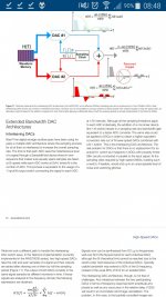
The interleaved dac structure is used in Tektronix' AWG's, see attached picture.
Link:
https://www.google.com/url?sa=t&sou...FjAIegQIBRAB&usg=AOvVaw39N4uCW5WZswm6aDcYkkv-
Looking at the picture it uses different physical dacs,1 for odd and 1 for even parts of the datastream. It seems the even order dac never spits out every other bit, demultiplexed.
Looking closer to the problems they faced, they may only be of interest for the extra bandwith they achieve by effectively doubling the bandwith, but I think it concerns all data.
I took your solution as resembling this structure, with the tight matching it needs.
Attachments
- Home
- Source & Line
- Digital Line Level
- My no DAC project, FPGA and transistors