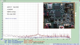
My no DAC project has achieved successful result after two months trial and error, though it's still under developing. I started to design 1bitDSM(no DAC) PCB to be able to have low noise floor fluctuation because it's relevant to SQ very much in my setup. THD has almost nothing to do with SQ. Theoretically speaking, the best solution to have low fluctuation is 1bitDSM, where no linearity is required in conversion from digital to analog. You can convert PCM into 1bitDSM(DSD) with hardware and make DSD into an analog signal with discrete parts. There are many ways to realize such DAC without a DAC chip. My attempt is FPGA and transistors to satisfy excellent performance which can compete with a modern commercial chip.
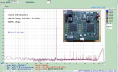
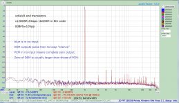
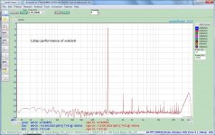
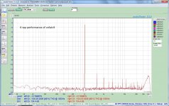
Two major strategies are mandatory to achieve the goal. FPGA and transistors with them can already outperform my DIYed 5bit DSM DAC, though the 1st pic is still an experimental result. THD+N is around 113dB, which is an almost impossible number for my 5bit DSM because it has a DAC chip(AD9717). The most challenging or impossible thing for a DAC chip is to have no noise floor fluctuation. I'm sure as long as a DAC chip has a resolution, even if it's 2bit, noise floor fluctuates as the amplitude becomes large. The 2nd pic is DIYed 5bitDSM(my 3bitDSM version also has the same plot). THD+N of 5bitDSM is around 110dB. If it wouldn't have a noise floor increase, you could have the same value as pic 1. THD is excellent because this is just after calibration. It matters little, and two or three days later you can't have the same number.
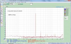
The 3rd pic is ES9038 made in eBay. This isn't a real performance of the chip since PCB is poor. If you use the chip at -0.1dBFS, the performance becomes far worse(the plot is at -2dBFS). Recent commercial chips usually don't have the best performance at fullscale. PCB construction is inevitably essential. I'm sure even carefully designed PCB can't remove noise floor fluctuation. So is AK4499. AK's homepage has two plots.
TECHNOLOGY | VELVET SOUND | AKM - Asahi Kasei Microdevices
One(the former) is at -155dBFS,the other(the latter) is at 0dBFS. You can see a moderate(6 to 8dB) noise floor increase. I would say low noise floor fluctuation doesn't exist in their to-do list.
1bitDSM itself has an ordinary performance like the 4th pic, though noise floor level and absolute THD are excellent. Small signal level(-28.35dB) prevents you from high performance. One of the two necessary strategies is analog FIR, which is used by pcm1792 in DSD mode. I haven't yet fully understood why it can increase signal amplitude without degradation of THD+N. It can magically boost the signal. S becomes large by analog FIR while THD+N is intact, where you automatically have a better performance like the pic1. The 5th pic is 6taps analog FIR. Noise floor and absolute THD is almost the same as 1tap. Only the signal does increase. The 6th pic is 12taps. The magic increases only the signal again.
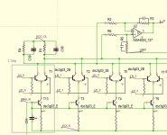
The rest of the two strategies is ECL like the 7th pic. If you replace T13 with a register, it's true ECL. T13 configured to constant current determines signal gain by T1. LN_0 and LP_0 are complementary 1bitDSM signal to switch two transistors of T1. When one is active, the other is inactive. Constant current defined by T13 passes through R4 or R1, where the digital signal(1bitDSM) is converted into an analog voltage. The significant advantage of ECL like conversion is PSRR. LN_0 and LP_0 are a dirty signal from the digital section. But the constant current of T13 is almost irrelevant to base voltage of two transistors of T1, which can result in noise-free transfer to the analog voltage across R4 or R1.
There may be several solutions to have isolation between the digital section and the analog one to have low residual noise. No DAC(1bitDSM) project usually has zero PSRR, where ends up less THD+N and prevents 1bitDSM without a DAC chip from the high-end application. If you have better isolation from the digital side, 1bitDSM can have high SNR. ECL is one of the strategies to make noDAC brilliant. ECL is easy to extend, i.e.,2taps,4taps, and more. The more, the better. The disadvantage is instability. It sometimes ends up an oscillation. I have now 24taps with moderate stability. I haven't yet fixed the oscillation problem. I'm not sure if I can have 32taps for further improvement. I'm still on the way.
The 8th pic is x128OSR in 8th order DSM. It has almost the same performance as x64. Noise shaping is, of course, better than x64. Xc6slx9 can have up to 5th order. More than 6th is done by external digital PCB(xc6slx25), which is the same one as my 5bitDSM DAC. The pulse train is transferred through an optical cable to keep high isolation. Onboard Xtal based OSC can successfully recover a clean clock(the 9th pic).
Two major strategies are mandatory to achieve the goal. FPGA and transistors with them can already outperform my DIYed 5bit DSM DAC, though the 1st pic is still an experimental result. THD+N is around 113dB, which is an almost impossible number for my 5bit DSM because it has a DAC chip(AD9717). The most challenging or impossible thing for a DAC chip is to have no noise floor fluctuation. I'm sure as long as a DAC chip has a resolution, even if it's 2bit, noise floor fluctuates as the amplitude becomes large. The 2nd pic is DIYed 5bitDSM(my 3bitDSM version also has the same plot). THD+N of 5bitDSM is around 110dB. If it wouldn't have a noise floor increase, you could have the same value as pic 1. THD is excellent because this is just after calibration. It matters little, and two or three days later you can't have the same number.
The 3rd pic is ES9038 made in eBay. This isn't a real performance of the chip since PCB is poor. If you use the chip at -0.1dBFS, the performance becomes far worse(the plot is at -2dBFS). Recent commercial chips usually don't have the best performance at fullscale. PCB construction is inevitably essential. I'm sure even carefully designed PCB can't remove noise floor fluctuation. So is AK4499. AK's homepage has two plots.
TECHNOLOGY | VELVET SOUND | AKM - Asahi Kasei Microdevices
One(the former) is at -155dBFS,the other(the latter) is at 0dBFS. You can see a moderate(6 to 8dB) noise floor increase. I would say low noise floor fluctuation doesn't exist in their to-do list.
1bitDSM itself has an ordinary performance like the 4th pic, though noise floor level and absolute THD are excellent. Small signal level(-28.35dB) prevents you from high performance. One of the two necessary strategies is analog FIR, which is used by pcm1792 in DSD mode. I haven't yet fully understood why it can increase signal amplitude without degradation of THD+N. It can magically boost the signal. S becomes large by analog FIR while THD+N is intact, where you automatically have a better performance like the pic1. The 5th pic is 6taps analog FIR. Noise floor and absolute THD is almost the same as 1tap. Only the signal does increase. The 6th pic is 12taps. The magic increases only the signal again.
The rest of the two strategies is ECL like the 7th pic. If you replace T13 with a register, it's true ECL. T13 configured to constant current determines signal gain by T1. LN_0 and LP_0 are complementary 1bitDSM signal to switch two transistors of T1. When one is active, the other is inactive. Constant current defined by T13 passes through R4 or R1, where the digital signal(1bitDSM) is converted into an analog voltage. The significant advantage of ECL like conversion is PSRR. LN_0 and LP_0 are a dirty signal from the digital section. But the constant current of T13 is almost irrelevant to base voltage of two transistors of T1, which can result in noise-free transfer to the analog voltage across R4 or R1.
There may be several solutions to have isolation between the digital section and the analog one to have low residual noise. No DAC(1bitDSM) project usually has zero PSRR, where ends up less THD+N and prevents 1bitDSM without a DAC chip from the high-end application. If you have better isolation from the digital side, 1bitDSM can have high SNR. ECL is one of the strategies to make noDAC brilliant. ECL is easy to extend, i.e.,2taps,4taps, and more. The more, the better. The disadvantage is instability. It sometimes ends up an oscillation. I have now 24taps with moderate stability. I haven't yet fixed the oscillation problem. I'm not sure if I can have 32taps for further improvement. I'm still on the way.
The 8th pic is x128OSR in 8th order DSM. It has almost the same performance as x64. Noise shaping is, of course, better than x64. Xc6slx9 can have up to 5th order. More than 6th is done by external digital PCB(xc6slx25), which is the same one as my 5bitDSM DAC. The pulse train is transferred through an optical cable to keep high isolation. Onboard Xtal based OSC can successfully recover a clean clock(the 9th pic).
Attachments
-
 xc6_x64.jpg366 KB · Views: 3,365
 -
 xc6slx_1.jpg437.8 KB · Views: 1,777
 -
 xc6_x128.jpg302.7 KB · Views: 1,681
 -
 dsd_42.jpg150.6 KB · Views: 1,645
 -
 xc_12tap.jpg321.9 KB · Views: 979
 -
 xc_6tap.jpg320.7 KB · Views: 2,946
 -
 xc_1tap.jpg319.9 KB · Views: 3,056
 -
 ESS_1kHz.jpg411.3 KB · Views: 3,139
 -
 AD9717_1k.jpg381.5 KB · Views: 3,216
Nice work ")
I've worked on a discrete DAC design so know how hard it is to get these results
I suspect your odd order distortion (3rd etc.) might be due to the poor Voltage Coefficient of the small 0603 Resistors you use in the DAC (R1 to R6)... Try replacing with a Larger (1206) Thin Film resistors and see if the 3rd harmonic reduces.
Last edited:
Thank you for your advice. I have never thought about the voltage coefficient of the register. I'm planning to use a high drivability differential amplifier like OPA1632 when I revise the PCB. ADA4898 is a little bit inferior to such op-amp. OPA1632 guarantees 600ohm load at 3Vrms. Theoretically speaking, it's better to use small register for Johnson noise. I was under the impression that such low noise was impossible in no DAC application. OPA1632 and large SMD could be the next step for further improvement. No DAC project is a pure analog circuit. I'm sure the PCB layout and the selection of components dominate performance.
I should point out first of all that like you have already said, I fully agree that THD has little if any impact to sound quality at these tiny levels, however as "Engineers" its important to understand the source of non linearity so we have a better understanding of the "systems" operation.
Ignoring the Digital noise sharpers, the noise of the 1bit DAC is dependent on :-
1. Jitter / Phase noise of the Clock (and isolation to this noise provided by the Relatching logic).
2. PSU noise on the DAC Array
3. Thermal noise of the components in the DAC array
4. Noise of the analogue circuit after the DAC Array.
I'm VERY surprised you are able to achieve these results without relatching after the FPGA, to remove the phase noise of the Spartans outputs. FPGA's I/O pin drivers are VERY dirty WRT Phase noise - being heavily correlated to the internal processing (A really really bad thing).
Relatching the FPGA outputs to your Master clock will bring huge sound quality benefits, but increase your design complexity.....
Using a balanced OPA such as the OPA1632 will resolve your even order distortion components, these are currently caused by the mismatch in current flowing though your DAC array as a result of your single ended output OPA (the current though your Inverting and non inverting paths is different, as the non inverting is referenced to Ground, while the inverting is referenced to an inverted signal on the output of the OPA, hence more current flows though this arm).
The trouble with the OPA1632 is that the noise performance via balanced outputs will be very good (about 132dB Awtd referenced to 2Vrms) - however the noise performance of its single ended output will be a little over 117dB due to the thermal noise of the effective 15K impedance of its internal feedback resistors (30K from each output phase) to the CM Diff amp.
In single ended operation this noise is purely "Flat" uncorrelated Thermal noise so is not subjectively bad, but it limits the "technical performance"...
TI has a later Fully DIff OPA the THS4551 and its internal CM feedback is reduced to an effective thermal noise source of 2.6K (see page 28 of the Datasheet), so SE noise performance will be improved to about 127dB.
Like THD, its the spectrum of the noise that's important - any correlated products are a big no no... so dont worry too much about nice / pure / clean / flat thermal noise even at 117dB its very low, the only issue is that it could be masking correlated components under the noise floor, and its my experience that we can hear correlated components buried quite deeply below the Noise floor.
If you know your noise spectrum is clean (as you would by looking at the differential outputs) then adding a flat noise is OK
I use OPA1632's on a budget discrete DAC where we dont have the space for a discrete OPA design - I'm OK with a SN of 117dB "flat noise" via the SE outputs, when I know its due 'ONLY' to 'clean' thermal noise, the DAC performance would otherwise be in the 130dB+ region (and is via internal balanced connections)
Ignoring the Digital noise sharpers, the noise of the 1bit DAC is dependent on :-
1. Jitter / Phase noise of the Clock (and isolation to this noise provided by the Relatching logic).
2. PSU noise on the DAC Array
3. Thermal noise of the components in the DAC array
4. Noise of the analogue circuit after the DAC Array.
I'm VERY surprised you are able to achieve these results without relatching after the FPGA, to remove the phase noise of the Spartans outputs. FPGA's I/O pin drivers are VERY dirty WRT Phase noise - being heavily correlated to the internal processing (A really really bad thing).
Relatching the FPGA outputs to your Master clock will bring huge sound quality benefits, but increase your design complexity.....
Using a balanced OPA such as the OPA1632 will resolve your even order distortion components, these are currently caused by the mismatch in current flowing though your DAC array as a result of your single ended output OPA (the current though your Inverting and non inverting paths is different, as the non inverting is referenced to Ground, while the inverting is referenced to an inverted signal on the output of the OPA, hence more current flows though this arm).
The trouble with the OPA1632 is that the noise performance via balanced outputs will be very good (about 132dB Awtd referenced to 2Vrms) - however the noise performance of its single ended output will be a little over 117dB due to the thermal noise of the effective 15K impedance of its internal feedback resistors (30K from each output phase) to the CM Diff amp.
In single ended operation this noise is purely "Flat" uncorrelated Thermal noise so is not subjectively bad, but it limits the "technical performance"...
TI has a later Fully DIff OPA the THS4551 and its internal CM feedback is reduced to an effective thermal noise source of 2.6K (see page 28 of the Datasheet), so SE noise performance will be improved to about 127dB.
Like THD, its the spectrum of the noise that's important - any correlated products are a big no no... so dont worry too much about nice / pure / clean / flat thermal noise
even at 117dB its very low, the only issue is that it could be masking correlated components under the noise floor, and its my experience that we can hear correlated components buried quite deeply below the Noise floor.If you know your noise spectrum is clean (as you would by looking at the differential outputs) then adding a flat noise is OK
I use OPA1632's on a budget discrete DAC where we dont have the space for a discrete OPA design - I'm OK with a SN of 117dB "flat noise" via the SE outputs, when I know its due 'ONLY' to 'clean' thermal noise, the DAC performance would otherwise be in the 130dB+ region (and is via internal balanced connections)
Last edited:
I'm VERY surprised you are able to achieve these results without relatching after the FPGA, to remove the phase noise of the Spartans outputs. FPGA's I/O pin drivers are VERY dirty WRT Phase noise - being heavily correlated to the internal processing (A really really bad thing).
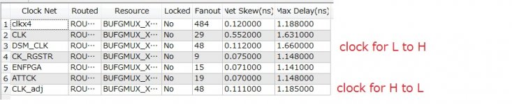
I agree with you that clock accuracy is critical to have high performance in DSM DAC. But I don't think external logic is better than FPGA I/O. FPGA I/O for driving ECL is output FF, neither internal FF nor LUT logic. Output FF is driven by an internal clock spine with less skew, which is almost impossible to have such an ideal clock by an external logic ic on the PCB. The attached pic is clock skew inside FPGA. Complementary DSM signal for LN_0 and LP_0 have the optimum phase relation, where good eye pattern isn't always the best. "CLK_adj," which is used for H to L, has a fine adjustment for the best phase relation. So, a max delay is not fatal but skew between 24taps must be minimal. If Skew is larger than 0.3ns, you can't have an excellent performance from my experience. It's probably OK if the skew is 0.112ns.
Another advantage of FPGA I/O is power voltage. My current version use LVCMOS1.5V I/O with 16mA capability. Another selection(SSTL or LVDS ) is sometimes the best. You can easily change output configuration by software.
If you design clock distribution circuit by external logic, you can have neither repeatability nor accuracy better than this. Furthermore, rerouting FPGA with different parameters can bring you a successful layout if your first try doesn't have a good result. It's an effortless task. But if you use external logic, rerouting means a redesign of PCB. That's why I don't think external logic is superior to FPGA I/O.
Attachments
Nice work indeed!
Maybe the oscillation problems are due to having to build the cml output yourself. OnSemi has a cml building block that might solve this:
NB4N11M: Multi Level Clock / Data Input to CML Receiver / Buffer / Translator, 2.5 Gbps, 3.3 V
I`ll be closely following this thread !
Maybe the oscillation problems are due to having to build the cml output yourself. OnSemi has a cml building block that might solve this:
NB4N11M: Multi Level Clock / Data Input to CML Receiver / Buffer / Translator, 2.5 Gbps, 3.3 V
I`ll be closely following this thread !
Last edited:
I'm a retired Audio IC designer so I fully understand the limitations of Silicon when operated in such phase noise critical applications.
Your confusing Skew with Phase noise - they are not related. You can have a bunch of outputs all perfectly matched edges - but this says NOTHING about there phase noise.
FPGA are sub optimal when it comes to I/O phase noise due to the challenges of internal power and clock distribution.
Imbalances in skew are compensated by balanced design of the DAC array.
Before we start pinging back and forth as to who is correct - I'll post a few measurement result of typical FPGA I/O phase noise.
In the test below, the FPGA (Spartin 6) is simply handling a 12MHz clock I/O Passthough via one LVDSI I/O pair (there is no other operation). The Signal is clean but already a very high Nosie floor.
Dropbox - 12MHz Single IO.jpeg
The second graph shows what happens with a second pattern is begin outputted on a second LVDS pair (the second signal is being gated on / off so you can see the effect on the FFT sweep) - you can see the cross induced phase noise modulation between these 2 I/O pairs.
Dropbox - 12MHz IO Isolation.jpeg
This is just a very simple demonstration - only 2 I/O pairs involved, with no "complex" operations being involved, just a simple Clock I/O flow through.... So one imagine the phase noise with complex operations and multiple I/O being performed when its THIS BAD with just two I/Os and no core operation.
Also, ECL is NOT the lowest low phase noise logic due to the low voltage level swings and small device geometry on the input devices of the Diff pair etc.
5V AC CMOS has significantly lower phase noise close to the carrier (basically across the audio bandwidth).
Here is a graph of logic family Phase noise:-
Dropbox - Logic Phase Noise.jpg
LVDS (not shown here) has REALLY poor LF phase noise.
I MUST stress again Output Skew has NOTHING = ZERO to do with I/O Phase noise, and its Phase noise we need to be concerned about when we are directly integrating the energy of output pulses.
Here is the Zoom FFT result of an old 1 Bit SDM discrete DAC array I designed (@ -20dB Ref 4Vrms Balanced as my measurement ADC introduces THD at higher input levels even with the -30dB Pre Notch Filter) - the discrete DAC array is based on CMOS TinyLogic, you can see a noise floor of -165dB with no visible THD....
I operated the Clock and TinyLogic on 6V rails to push the Dynamic range performance
Dropbox - Discrete SDM Array -20dB Zoom FFT.jpg
On the FFT above, the spuire below 1KHz are due to mains related hum - 50Hz / 100Hz products magnetically induced into the measurement setup / lab bench.
Last edited:
For the simple tests above, the measurement was made on the FPGA LVDS outputs via a LVDS to CMOS translator (Diff to SE) powered from a clean supply. The LVDS RX has lower close in phase noise then say a TEK P6248 Diff Probe - Active DIff probes are designed for speed rather then PN performance and tend to bottom out around -100dB to -120dB.... (They are really noisy at close carrier offsets).
While the test above was made with a Agilent system, I also have a Wavecreast SIA4000 PN measurement system that has Diff inputs and using passive Diff probes confirms much the same results. I tend to use the Agilent system more as I can directly dump data via GPIB to a PC and its besides my lab bench position...
But for sure, Diff outputs will help with AM to PM conversion but real life CM rejection is really not that good at such high edge speeds at the best of times, with a discrete Diff stage is going to be even harder to get effective CM rejection... Track pair Impedance matching on the PCB with physically small IC's is hard enough, PCB layout with a discrete design would have to be a work of art to achieve decent CM rejection - beyond say 20dB or so at these edge speeds.
I'm guessing that within the FPGA, the signal is routed as "single ended wiring" - I'm really not aware of differential signalling within the Spartan core (beyond the I/O Pads), so the damage to PN is already done before its converted to external Diff signals.
Its a 10 minute job for me to hook-up a PCB if somebody wanted test there design - easiest is to look at a clock output pair on the same I/O bank as the DAC Array outputs to get a picture of PN on the FPGA I/O.
Last edited:
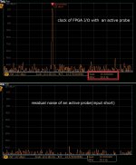
OK, so you did clip off amplitude noise. I'm surprised that your active probe works poorly at close carrier offsets, as I would expect an active probe to produce additive noise. Apparently it is nonlinear enough to have some mixing effect going on between its low-frequency noise and the carrier.
Active probes are designed for greatest B/W, so feature the smallest possible geometry devices on the input stage (Lowest IP capacitance = Highest B/W).
The Close-in noise of active probes when used in there linear range is purely thermal/ shot noise, nothing to do with "mixing effects"... just as with any Diff stage when operated in its linear range...
Active probes also have Highish value series resistors internally to help limit the current into the protection circuits during over-voltage events - these series resistors also add noise...
As would be expected we find slower active probes have better close in noise performance - we put this down to maybe larger input devices...
As I mentioned, where Phase Noise is really critical then we use passive Diff probes if circuit loading conditions allow... On some designs we have a pair of SMB positions on clock line on the PCB to facilitate PN measurements - thus avoiding noise issues with Diff probes.
We have a selection of Active High speed diff probes from Agilent / Tek from 1GHz to 12GHz and non standout as better or worst then others, but the general rule is lower B/W, better close in PN...
Last edited:
The Close-in noise of active probes when used in there linear range is purely thermal/ shot noise, nothing to do with "mixing effects"... just as with any Diff stage when operated in its linear range...
Then why isn't it additive?
Nice work indeed!
Maybe the oscillation problems are due to having to build the cml output yourself. OnSemi has a cml building block that might solve this:
I guess the oscillation is due to many differential amplifiers(24taps). It becomes unstable when the DSM signal changes its state(H to L or L to H), where both transistors are simultaneously active. It automatically stops the oscillation when both are not in an active state.I haven't yet found an effective way to stop the oscillation.
Would you mind sharing the resistor values for R1 to R4?
No problem. R4=15,c39=5p,R1=15,C38=0,R2=R6=150,R3=R5=680//4700p.But they are subject to change since the circuit is under developping. OPA1612 is more prefferable than ADA4004 or ADA4998.
Your confusing Skew with Phase noise - they are not related. You can have a bunch of outputs all perfectly matched edges - but this says NOTHING about there phase noise.
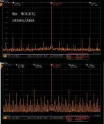
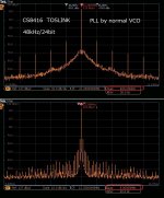
Yes, I agree with you that both are a different matter. I'm not pessimistic about FPGA jitter because my measurement is relatively positive, though my measurement environment isn't ideal. The 1st pic is the famous jittery clock, IIS of Rpi(MDO3102 and TAP1500). I can't believe it can be a DAC clock. But as long as your DAC is multibit, this doesn't have fatal degradation. If your DAC is DSM, your noise floor could be around 16bit resolution. The 2nd is SPDIF recovered clock by CS8416. Harmonics of 48kHz is due to 48kHz sampling. This is also not excellent.
The 3rd pic is the clock of my 1bitDSM board. This is after two I/Os because the clock passes through another FPGA before it arrives the 2nd FPGA which has DSM process and transistor drivers. It's not perfect but far more better than the 1st pic and the 2nd. I'm on the application side, not on the manufacturer side. What I can say is how much jitter is acceptable in a particular application. FPGA jitter in not ideal condition doesn't have fatal degradation on DSM at least up to x128OSR as long as I have experienced.
Another example for FPGA jitter is DDR3 application. This is a guideline for DDR3, where you need excellent jitter performance since it has 800MHz clock at max.
https://china.xilinx.com/support/documentation/white_papers/wp479-ddr3-si-pcb.pdf
It shows some eye pattern with jitter. When your DDR3 application has a successful result, FPFA I/O must satisfy the requirement of DDR3. Spartan6 can handle DDR3 interface, though you need careful consideration to implement it into FPGA, including PCB layout. Tha's why I'm sure jitter of spartan6 is acceptable in DDR3. So is in x128OSR DSM
Attachments
I guess the oscillation is due to many differential amplifiers(24taps). It becomes unstable when the DSM signal changes its state(H to L or L to H), where both transistors are simultaneously active. It automatically stops the oscillation when both are not in an active state.I haven't yet found an effective way to stop the oscillation.
Thanks! That clarifies a lot. The onsemi building block (do check it if you haven't yet pls), is basically what you built but monolithic: so you don't have to fiddle with current sources, and you keep control over r1 etc, because it has an open drain/collector output.
This might very well solve the oscillation problems, while you don't lose functionality and have better matching etc.
To xx3stksm & MarcelvdG:
I'm thinking that all JohnW is trying to say is that if the reclocking after the fpga's are left out, all someone else needs to do is copy xx3stksm's basics, add some flip flop's, claim better performance and all your time and effort has been for someone else's fame and fortune. That's low hanging fruit there that needn't nor shouldn't be there, except for blind faith in fpga building blocks.
I'm thinking that all JohnW is trying to say is that if the reclocking after the fpga's are left out, all someone else needs to do is copy xx3stksm's basics, add some flip flop's, claim better performance and all your time and effort has been for someone else's fame and fortune. That's low hanging fruit there that needn't nor shouldn't be there, except for blind faith in fpga building blocks.
That's why I'm sure jitter of spartan6 is acceptable in DDR3. So is in x128OSR DSM
An easy assumption to make, but what is important is the frequency content (Spectrum) of the PN.
Communications / Data systems set there PN measurement corner frequency too high for audio applications - typically 12KHz or higher, making there Jitter specs. useless for audio applications - most systems have VERY poor close in phase noise due to high PLL BW, poor oscillator Q, noisy low power logic design, etc.
If you look at the PN performance of Logic family's I attached ealier you can see that ECL has worst Close-in Phase noise compared to most CMOS family's, bench testing shows LVDS is even worst.
To get a better understanding of the "ball park" Jitter performance we require with Simple Maths (There are many factors that determine the absolute jitter requirement, but such basic math gets us more or less in the correct "Decade"):-
1 bit SDM at x128 FS= 5.6448MHz = 177nS
Lets set a target of 120dB Dynamic range (1 millionth), so we need to be able to reproduce our pulse stream with a short term timing accuracy of 177nS / 1,000,000 = 177fS
177fs assumes 100% modulation, at max we have say 50%, so:-
177fS/2 = 88fS
88fS is a crude "Off the cuff" calculation and does NOT take into account many details, but its a good starting point to appreciate the Jitter requirements to achieve 120dB DR with a pure 1bit system at 128FS...
Moving average DAC array arrangements / higher SDM bits ease these PN requirements, but thats getting into the finer details...
The point is you need to forget shooting for pS short-term jitter performance, but you need to be in the low fS range...
"Short-term" means over say 5 - 10 seconds to bring the Close-in noise slope (area) down to a decent level...
What I'm trying to impress upon you is that the typical Jitter performance corner frequency spec'ed from 12KHz is useless for our discrete Audio DAC array applications - you need to be thinking about timing accuracy in a different realm to normal industry standards (In B/W and level).
Measuring Close in Phase noise with the required Dynamic range is extremely difficult and expense - when higher performance measurements are required, we have a whole RACK of computer controlled equipment to performance the task, but the system still sets the industry standard for close in Phase noise measurements (the system has been upgraded since the picture was taken):-
Dropbox - Phase nosie measurement system.jpg
Heres the systems confidence test (basically the systems Noise floor):-
Dropbox - Agilent E5500 System Confidence Test.jpg
(Again the Mains related spuire is due to magnetic coupling of background fields into the system).
I said once before here on this forum that working with Discrete SDM DAC design is frustration but also the most educational experience a "Digital" audio designer can undertake
I designed my first commercial discrete SDM DAC back in 1990/1991 (Pink Triangle Dacapo) and still to this day rely on the design fundamentals I learnt back then. I can honestly say that as a Digital audio designer, its was the most concise learning period of my whole career
Last edited:
Thanks! That clarifies a lot. The onsemi building block (do check it if you haven't yet pls), is basically what you built but monolithic: so you don't have to fiddle with current sources, and you keep control over r1 etc, because it has an open drain/collector output.
This might very well solve the oscillation problems, while you don't lose functionality and have better matching etc.
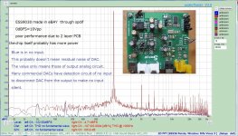
Thank you for the feedback. I also googled several monolithic modules to eliminate the complexity of discrete components. What I did consider was the noise power of the current source. NB4N11M has 16mA one(fig.18). The current has no PSRR like power rail of Signalyst topology. You usually can't predict how much noise power it has. The only way to control the noise power is a simple current source by a transistor as I posted before. Base voltage(BIAS_N) driven by LT3042 is the major factor to determine the noise power. If you fail to select a clean current source, your prototype PCB becomes a mess. Discrete components are inconvenient but have flexibility. That's the very reason why I chose discrete transistors in my first try. After two months of struggle, I can say now it's not a bad selection. It has very low noise power because of LT3042 and easy to change the current(from 3mA to 5mA is optimum). I would say the oscillation is a trade-off for low noise power.
- Home
- Source & Line
- Digital Line Level
- My no DAC project, FPGA and transistors