If a monolithic design is possible, using Darlington transistors seems to be an effective approach. When working with discrete components, space constraints often mean it's preferable to use as few elements as possible for each tap. Shorter wiring for the common collector connection also matters. Due to wiring length limitations, the max tap count is 32.
Therefore, it appears that single transistor switching could be favorable for the overall performance. The variation in Vbe has a more significant impact on switching precision than β, making it challenging unless characteristics can be closely matched, which isn't achievable in a discrete design.
Therefore, it appears that single transistor switching could be favorable for the overall performance. The variation in Vbe has a more significant impact on switching precision than β, making it challenging unless characteristics can be closely matched, which isn't achievable in a discrete design.
I'm not familiar with FETs, but it seems that the gate voltage required to turn off a JFET might be higher than that of CMOS. When considering switching applications, CMOS might be more suitable. However, transistors can be completely cut off with a Vbe (0.7V) or higher, whereas CMOS might require around 3V. Since there's no need for current flow, the actual circuit experimentation will determine the outcome. Given that 3V can be directly driven by an FPGA, it's worth trying out. With no base current, complete switching is achievable. The variation in cutoff voltage could be an issue.
至CMOS转
why could omultiple taps share one resister ?Hi, Zoran. I'm afraid I misunderstand what you mean. But I think your schematic requires accurate resister matching. The advantage of 1bit DSM is no need to care about resister matching. The attached pic has one resister for transistors; R4 for negative ones and R1 for positive ones. One resister is the essential point of 1bitDSM. Each tap doesn't have the same current(almost 0.1% accuracy). But the imperfectness results in a slight frequency response error, doesn't mean distortion.
The circuit diagrams of a 16-bit R2R DAC and a 1-bit DAC with 16 taps are similar, but the characteristics of the former depend on the precision of the resistors, whereas the latter does not. Additionally, the 1-bit DAC requires only a single resistor. In circuits that can output both, when operating as a 1-bit DAC, it should function with just one resistor.
第二张图片是一个基本单元,一个水龙头。如果你想测量超过36dB的SNR,我相信你需要一些补偿来消除ADC的残余噪声,除非你有像AP这样昂贵的噪声。我的ADC(两个AD48)的残余噪声几乎为-24dBFS。如果您的 DUT 也是 -36dBFS,您可以得到的是总和的平方根:-12dBFS。如果 DUT 为 -48dBFS,则为 -3dBFS。这是一个粗略的估计,但很实用。一个抽头大致具有-2dBFS,这几乎是低噪声运算放大器应用中的最佳数字。换句话说,One Tap没有与DSM相关的降级。如果能有一个理想的模拟FIR电路,最好的SNR是120dB。当然,这在模拟域中是不可能的:虚数。
第三张图片是7960个水龙头,其中模拟FIR几乎是理想的。补偿SNR(123.123dB)非常好,因为这是由分立元件完成的。如果您想要一个更正确的数字,您应该使用陷波滤波器补偿 THD。我不是THD的人。补偿仅适用于 SNR:SNR 人员。
您在数字领域
did ADC use in SDM feedback loop ?没问题,我的座右铭是“没有ADC,没有DAC”,为DIYer拥有一个AP产品并不容易。但DAC性能与ADC成正比,特别是当THD超过-120dB时。AD7768-8可能是可靠的,因为它们中的每一个(8个ADC)具有几乎相同的THD性能。一个ADC和两个ADC测得的THD没有区别。频率范围内的THD有点棘手,因为我的DAC接受由传输或ADC馈送的优化光信号。两者都只有有限的实际使用频率。从图187到图375,它们是750Hz,999Hz,1Hz,5Hz,3.6kHz,12kHz,999kHz和96000kHz(32768Hz=(341/1)* 8)。最大摆幅为10Vpp(差分),但-3dBFS(7Vpp)实际上是最大振幅。如果您的DAC超过7Vpp,则需要有一个电阻分压器。
它们的本底噪声没有得到补偿。您可以使用两个ADC(-120.3dBFS,图9)的残余噪声来补偿该值,尽管可能存在一些误差。如果使用 8 个 ADC,则可以产生 -127dBFS 残余噪声,比 2 个 ADC 更精确。
")
I'm not familiar with the term "SDM feedback loop," but specific frequencies are intended to send a test signal from the ADC, performing synchronized sampling and aligning it with the FFT bin. This allows the omission of window functions, resulting in the most accurate values. For instance, 1500=(96000/32768)*512 and 999=(96000/32768)*341.
theoretically,1-bit DAC need only one taps ,why do 1-bit DAC need 16 taps?The circuit diagrams of a 16-bit R2R DAC and a 1-bit DAC with 16 taps are similar, but the characteristics of the former depend on the precision of the resistors, whereas the latter does not. Additionally, the 1-bit DAC requires only a single resistor. In circuits that can output both, when operating as a 1-bit DAC, it should function with just one resistor.
You can make a FIRDAC when you use more than one tap. The taps then get delayed input signals and their output signals are added, turning the whole thing into a mixed-signal FIR filter. It reduces the sensitivity to far-off phase noise and spurious tones on the clock and it does a part of the reconstruction filtering.
The characteristics of a 1-tap 1-bit DSM are not excellent. To address this, when adding a 16-tap(each has one clock delay) in the analog domain, it provides the same functionality as a 16-tap moving average digital filter. Although not possible in the digital domain, such addition can be accomplished in the analog domain. If analog switching is flawless, this operation would result in a 16 = 2*2*2*2 = 4*6dB = 24dB improvement in SNR.
Achieving similar effects can be done by parallelizing the DAC outputs, but in that case, the improvement would be 12dB instead of 24dB. The same goes for ADCs, resulting in a 12dB enhancement. Such analog-domain moving average filters work quite efficiently, almost like magic. THD is significantly improved as well because individual distortions are averaged out. This improvement depends on the order of taps. When implementing the digital side in an FPGA, you can set up internal registers for rearrangement and adjust them to achieve the optimal state. With perfect switching and optimal tap arrangement, you can achieve SNR exceeding 120dB and THD below -120dB.
However, at this level, 1-bit DSM faces issues with repeatability and doesn't consistently maintain these figures when you build multiple units for a multi-system setup. Surprisingly, the solution is to employ 2-bit DSM. While 2-bit DSM faces linearity issues, the middle point "00(zero)" between "01(max positive)" and "11(max negative)" can be digitally adjusted, determining symmetry between the positive and negative sides. This adjustment has the same meaning as tuning for second-order distortions. By incorporating some registers within the FPGA and setting optimal values for each board, you can achieve 120dB SNR and -120dB THD consistently and with less power compared to 1-bit DSM.
One shared register is the same load of each tap to construct an FIR filter in the analog domain.why do multiple taps share one resistor?
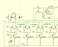
I can't download Discrete DAC Stg6.png,please upload it to this thread,thank you!So we are do things rather different, using CMOS logic as it has lower Phase Noise, and higher voltage swings.
In the attached image you can see a development PCB we are currently working on with a simple SDM discrete DAC array and FPGA modulator (Digital filtering is performed by the large XMOS which also supports MQA unfold, USB and System control etc).
This design has a galvanically isolated analogue stage, not because it helps measurements, but because in practical use isolating the USB Host ground from the Analogue system saves a whole bag of hurt with hum loops etc..
The Discrete clock stage is located between the discrete DAC arrays for shortest signal path, the SDM signals from the FPGA are resynchronized to this MASTER clock, before being fed into the DAC array.
The clock is isolated and fed back to the Digital section / FPGA / XMOS etc.
The clock circuit has an ultra low noise semi discrete regulator. Due to space constants, the DAC arrays are powered via an ES9311 Low noise regulator. If space allowed we would have preferred to use a semi discrete regulator design as used for the Master clock - but the ES9311 is not that bad, importantly in can be designed to provide "active" regulation across the whole audio B/W which is very important to avoid "capacitor sound"...
The resynchronization stages have there own regulators and LC networks to help isolation between stages.
The two transformers provided very low noise isolated supply to each channel - these are synchronized to the Audio master clock (the low Phase noise provides a low noise DC output) to prevent unwanted noise products folding back into the audio band, and despite there size they can provide 1.5A each! - infact all switching supplies in the digital section are also synchronized to the audio master clock.
The DAC array supports SDM to x512, so native DSD can be routed to the DAC array without re-modulation.
Dropbox - Discrete DAC Stg6.png
- Home
- Source & Line
- Digital Line Level
- My no DAC project, FPGA and transistors