WARNING: This thread had a tortuous start during the initial four weeks. Therefore, new readers are invited to start from this recap post, which should save them a lot of frustration. Curious readers can then go back to the earlier posts in order to get a sense of how we got there in the first place... I hope you enjoy the ride!
###
I am currently working on a modular audio interface with the following specs:
- Dedicated ADC board powered by 1 × XMOS XUF232-1024-FB374 (isolated)
- Dedicated DAC board powered by 1 × XMOS XUF232-1024-FB374 (isolated)
- 8 × balanced mono inputs (XLR or mini XLR, TBD)
- 8 × balanced mono outputs (XLR or mini XLR, TBD)
- 8 × AK5578EN 32-bit, 768kHz, 130dB ADC chips in mono mode
- 8 × AK4499EQ 32-bit, 768kHz, 140dB DAC chips in mono mode
- 192 × OPA1612 Op Amps for input channels
- 64 × OPA1612 Op Amps for ouput channels
- TOSLINK S/PDIF + ADAT Input
- TOSLINK S/PDIF + ADAT Output
- 5-pin LEMO Jack Clock Input
- 5-pin LEMO Jack Clock Output
- CC-BY-SA-3.0 Open Source License (Hardware + Software)
I am making good progress, but I have a few questions:
# Op Amp Selection
- Is the OPA1612 the best option?
- Would the OPA2156 CMOS be a better alternative?
- Should I give the mysterious RT6862D/RT6863 of the Khadas Tone Board a shot?
# Input Buffers Design
I am designing the DAC board following AKM's reference design, which is making things pretty straightforward. Unfortunately, the ADC reference design is using the obsolete NJM5534. Where could I find a reference design for an ADC input buffer using the OPA1612 or any pin-compatible Op Amp?
# Connectors
For many applications, the small footprint of the mini XLR connector is really attractive. Unfortunately, it is more expensive, less reliable, and less versatile (male versions cannot be found in certain for factors). Therefore, I am inclined to mount the input and output connectors on separate boards. When doing so, how should I design the connection between these connector panel boards and the ADC and DAC boards?
# Shielding
Should I shield the ADC and DAC chips? If so, which other passive components should be covered by the shields?
Just for kicks, these interfaces will be connected to a Xilinx XCZU15EG-2FFVC900I FPGA with 3,528 DSP slices for low-latency/low-jitter sound processing, using an Enclustra ME-XU7-15EG-2I-D12E System-on-Module mounted on an Enclustra Mercury+ PE1-300 base board. And for the user interface, I will use a Khadas Edge mounted on a Khadas Captain. All this goodness will be released under CC-BY-SA-3.0 as well.
Last edited:
...The DAC board will use 8 × OPA1612 op amps per mono channel (64 op amps in total), following the ...
That looks like the wrong reference design for use with AK4499. It's different from the earlier AK44xx chips in multiple ways, current out instead of voltage out is a big difference, as one example.
Last edited:
That looks like the wrong reference design for use with AK4499. It's different from the earlier AK44xx chips in multiple ways, current out instead of voltage out is a big difference, as one example.
I am using the reference design provided on Figure 83. External I-V Conversion Circuit Example (Mono mode), page 110 of the 019001308-E-00 document provided by AKM upon registration for the AK4499EQ.
I don't understand why would you use a $2000+ dollar Zynq. The whole point of a Zynq is to have full ARM CPUs integrated (Cortex A53 in this case), and I don't see how you are using that? You're also adding another ARM SBC on top of it just to drive a front panel, which the Zynq is already overkill for?
The BOM cost for this will be astronomical. As you currently have it specified, at least $1000 in op-amps, $2000 for FPGA board, $400 if not more for the AK4499s alone based on AK4497 pricing.
The BOM cost for this will be astronomical. As you currently have it specified, at least $1000 in op-amps, $2000 for FPGA board, $400 if not more for the AK4499s alone based on AK4497 pricing.
Any idea where I can find more information about it?
You would have to talk to the AKM wholesale distributor for your sales region. Depends on whatever they might be willing and or able to do for you. The rev 0 board is a pre-release version.
I don't understand why would you use a $2000+ dollar Zynq. The whole point of a Zynq is to have full ARM CPUs integrated (Cortex A53 in this case), and I don't see how you are using that? You're also adding another ARM SBC on top of it just to drive a front panel, which the Zynq is already overkill for?
The BOM cost for this will be astronomical. As you currently have it specified, at least $1000 in op-amps, $2000 for FPGA board, $400 if not more for the AK4499s alone based on AK4497 pricing.
The BoM is just shy of $4,000, including quite a bit of USB glue between the different components. The big FPGA is there for sound synthesis and sound effects. I am trying to bring the analog components of Eurorack synthesizer modules into the digital domain, while bringing the sound effects of DAWs on silicon, considering latency as enemy #1. All the while, I am trying to make modular synthesizers and control surfaces a lot more modular, using USB 3.0 as primary fabric for a LEGO-like system.
The ARM SBC is added to the mix because it is cheap (less than 10% of the total BoM), while providing many useful interfaces, especially with respect to displays and cameras. I do not want to build all this from the ZYNQ SoM, and I certainly do not want to build my own ZYNQ base board... If you were to take 8 of these systems, you'd get something that is 5 times less expensive than any comparable setup, but with 10 to 50x more DSP power...
You would have to talk to the AKM wholesale distributor for your sales region. Depends on whatever they might be willing and or able to do for you. The rev 0 board is a pre-release version.
Thank you for this. I will get in touch with them right away! Fingers crossed...
I don't understand why would you use a $2000+ dollar Zynq. The whole point of a Zynq is to have full ARM CPUs integrated (Cortex A53 in this case), and I don't see how you are using that? You're also adding another ARM SBC on top of it just to drive a front panel, which the Zynq is already overkill for?
The BOM cost for this will be astronomical. As you currently have it specified, at least $1000 in op-amps, $2000 for FPGA board, $400 if not more for the AK4499s alone based on AK4497 pricing.
Also, you can cut the BoM in half by using a cheaper SoM. For example, the SoM with ZYNQ 7030 is only $150. Also, the current $4K BoM includes a $169 Samsung PM851 1TB attached to the SoM and a $490 Samsung SSD 970 EVO 2TB attached to the SBC. Remove these and the BoM goes below $1,500, which is quite affordable for an 8+8 ADC/DAC interface with mono chips on both ends.
Yes, this is an ambitious project, but I am going at it in small increments (see below).
There are many reasons why using a ZYNQ makes sense:
# Floating-Point Operations
The LuTs and DSPs of a traditional FPGA are really bad at dealing with floating point operations. Of course, you could put a few soft cores in there, but this would be a massive waste of resources. Instead, you're much better off delegating all your floating point computation to the ARM cores found on the SoC. Granted, you could run these on the ARM cores of the SBC, but they are far away, and these are not real-time cores.
# Real-Time Cores
Alongside the four Cortex-A53 cores, the ZYNQ includes two real-time Cortex-R5 cores. These can be used for real-time coordination across multiple subsystems, thereby making a great contribution to latency reduction.
# Interfaces
Using a SoC instead of a plain FPGA gives you many more interfaces to play with. Granted, you could add some of these in the form of IP on the FPGA, but it would dramatically increase your development costs, while again leading to a massive waste of precious FPGA logic.
# Availability
While you could theoretically get a bigger FPGA (more LuTs and DSP slices) by eliminating the ARM cores, you will actually find it difficult to source these components in low volumes, simply because more and more people are moving to SoCs.
This is especially true for FPGAs/SoCs that are mounted on off-the-shelf modules. If you were to buy the XCZU15EG SoC from Digikey directly, it would cost you more than $6K. But assembled as a module, Enclustra will happily sell it to you for $2K. And you can still buy a pin-compatible module with a 7030 for $150. This makes your design super scalable from a performance/price standpoint.
Now, this begs a few questions. For example, why not using the SoC alone, thereby getting rid of the SBC? This would simplify the design quite a bit, but there are a few reasons why I decided to go this way:
# Roadmap
The SoC (base board + SoM) will actually be the last component of the architecture. I will first start with the SBC connected to a USB hub of my design (more on this later). I will then add the ADC board, which is using a slightly more mature chip than the DAC board. After that, I will add the DAC board, and this will give me a first version of a complete system. The SoC will be added last, as an option. This will ensure that the most expensive and most complex components of the build are only added toward the end, once a lot of experience has been gained and the design has been refined enough.
# User Interface
Most high-performance FPGA-based SoMs are not geared toward user interface applications. Therefore, adding things like displays, microphones, buzzers, gesture cameras and the likes is difficult and expensive. On the contrary, ARM-based SBCs like the Khadas Edge come pre-built with all that goodness. The $49.90 5" 1920 x 1080 touchscreen is a great example. Therefore, the SBC will be used for the user interface, while the SoC will be used for signal processing.
# Real-Time Processing
By enforcing such a strict separation of duty between the SBC and the SoC, I will ensure that any slowdown of the user interface does not affect the sound signals. In other words, 100% of the sound processing will take place within the SoC and the ADC+DAC boards, never transitioning through the SBC. This is important, because the SBC will be doing quite a bit of rendering on the UI side (think about the kind of UI provided by the SERUM software synthesizer).
For example, if an audio effect requires the synthesis of a sound using custom wavetables, these wavetables will be configured on the SBC, computed on the SoC, then displayed back on the SBC. But by the time this display took place, the sound has already been generated by the SoC and played through the DAC.
Obviously, this makes for a much more complex software architecture, but software is my background, and this part does not scare me at all. I wish I could say the same about input buffer design... ;-)
# USB Hub
The USB hub will be used to connect 8 SBCs together. It will be constructed around the USB5807 chip. This will make for a total of 64 audio inputs and 64 audio outputs. This USB hub will also be responsible for providing 24 additional USB 3.0 ports for each SBC. These will be used for connecting what I call Eurobrick modules, in a fashion similar to what Special Waves is doing, but with a much wider range of bricks.
# Eurobricks
But instead of having just buttons, encoders, and faders, you'll also get jacks for audio inputs/outputs and CV ports. Each brick will include an ATmega328 microcontroller. CV inputs will be implemented using the microcontroller's ADC inputs, while CV outputs will use a simple shift register. In other words, the CV ports will be real.
The audio inputs/outputs are a different story though: these will use XLR (or mini XLR) ports on the back, but they'll be exposed as "virtual" inputs/outputs through "real" 3.5mm jacks on the front. In other words, such a jack will not carry any audio signal. Instead, it will just carry an identifier for an audio signal, thereby allowing the user to perform a logical patch through a physical jack. Therefore, composers will be able to patch audio inputs/outputs as if they were using an analog modular synthesizer, but everything will remain in the digital domain. This will preserve the mechanical nature of modular synthesis, while allowing patches to be re-created at the press of a button. In other words, you get the best of both worlds.
Most bricks will be small single-unit 43mm × 43mm components, making the system very modular, but some will be larger. For example, the motorized fader brick will be a 1 × 4 component including a PGFM3200 100mm motorized fader and an AS1101P-1004F 101 segments 100mm colored bargraph module. This should allow users to create control surfaces as simple as an AVID Artist Mix, or as complex as a Pro Tools | S6.
# AVB
Thanks to the XMOS chips used on the ADC and DAC boards, I will get Gigabit Ethernet AVB ports as well (one on the ADC and one on the DAC).
# Dante
The FPGA fabric of the SoC and the two Gigabit Ethernet ports of its base board will be used to provide two Dante ports. This will allow the system to provide both AVB and Dante ports at the same time, across two separate networks. This part will require a non-open-source IP from Audinate though.
# Battery Power
Last but not least, the whole platform is designed in such a way that it can be powered by built-in batteries. Each module has a 430mm × 129mm footprint with four separate batteries (one for the SBC, one for the ADC, one for the DAC, and one for the SoC). A full 8-module system will have a 1,032mm × 430mm footprint, but it will come in 8 separate modules that are easy to carry around.
Just for kicks, such a setup would include:
- 8 × 5" touchscreens
- Eurobrick replicas of most Mutable Instruments modules
- 54 × 3.5mm patching ports
- 16 × motorized faders with 16 × 101 segments bargraphs
- Full hardware interface for SERUM
- 128 pads monome sequencing grid
- 24 key LUMI keyboard
- Full-size QWERTY keyboard
- Trackpad
- Jog wheel
And up to 28,224 DSP slices for more sound effects than anyone should ever need...
Here is a Google Sheet describing all this in more details.
The PCBs will be designed using KiCad. The user interface will be designed as a web application running on the SBC, with HTTP endpoints served by the SBC and the SoC. This should make the development of custom software modules a lot more accessible to a wide community of developers.
Last edited:
Yes, this is an ambitious project, but I am going at it in small increments (see below).
I can see you've put a lot of thought into it. The Cortex A53s will give you good performance, especially if you can use libraries that have NEON intrinsics, but will that bottleneck you? I guess you are doing some of the DSP via FFT on the ARM and some in the FPGA with the DSP slices? I must admit I am not too familiar with DAW / pro audio software, so I don't know the requirements exactly.
There is a non-audio project I am working on at work that has a lot of similar architectural principles, but we have a small team, not just one person. If you can pull this off it will be impressive.
While the hardware part of the project is certainly no walk in the park, the most challenging element will probably be the development of sound processing logic on the FPGA fabric, using off-the-shelf IP cores provided by Xilinx under an End-User-License-Agreement (free but not Open Source). This is similar to what was done for the Waldorf Kyra (all by one person as far as I can tell). And the real challenge will be to develop this logic and its software glue in such a way that it could be used by the large number of DAW applications currently available on the market. I have yet to figure that part out...
And to be clear, all the sound processing will happen either in the XMOS chips (easy to program in C/C++) or in the FPGAs of the SoCs (using LuTs and DSP slices). The ARMs won't do any signal processing directly, but they'll contribute to it, by generating wavetables for example.
Yes indeed, this is an ambitious project, but it's a lot of fun...
I should also answer another question: why making the ADC and DAC boards so positively overkill by using the ADC and DAC chips in mono mode? Even the top-of-the-line Merging Horus does not do that!
To this question, I have no rational answer besides the fact that nobody seems to have done it yet, and there is no point redoing what has already been done. Also, because everything else about the proposed platform is so obviously overkill, why not going all the way?
Of course, using one ADC or DAC chip per mono channel is only part of the challenge. Designing proper power supplies and clock lines won't be easy either. And getting all the components properly isolated and shielded will add to the fun as well.
Can all this be done by a single person? Probably not, but such is not my goal.
So wish me luck! Or even better: help me out! (^_^)
I see. Well, if you're spending this much money on the processing and other parts, then I guess there's no reason not to use 8 AK4499, etc. Merging probably wants to hit a price point, plus at some level it just becomes bragging rights ") .
.
I'm afraid I probably don't have time to contribute (I have my own unfinished projects that stretch back 5 years now), but I definitely wish you luck!
. I'm afraid I probably don't have time to contribute (I have my own unfinished projects that stretch back 5 years now
), but I definitely wish you luck!Thank you! It is most definitely about bragging rights. We all want to pump the volume up to 11, don't we?
For the record, I should mention that this is not my first attempt at this. Four years ago, I came up with a first design for something along the same lines, but without the Eurobrick concept (I really did not understand modular synthesis back then). The project remained on the drawing board, but it lead me to create a company that now makes a PCI board with 16 × Xilinx XCZU15EG SoCs and 64TB of flash with 85GBps read/write bandwidth (B as in Byte, not bit). In other words, flash that is faster than SDRAM, just because we used all the transceivers of the FPGA fabric as a way to drive the flash in a massively parallel fashion. Therefore, while not being an FPGA expert myself (again, I'm mostly a software person), I have access to real experts if (when) the need arises.
This time around, I think my design is a lot better, and I am taking an open source approach, because this is where hardware is going now. Also, the project's success is predicated upon the adoption of the Eurobrick format that I am working on, therefore it makes sense to go open source for the whole thing.
The rest of the system is mostly designed as a showcase, demonstrating how this Eurobrick form factor could be used to quickly design professional audio processing tools. Therefore, the better the specs, the better the showcase.
In order to get a better idea of how the system works, here is the stack of PCBs that will be used. The USB topology is quite complex and remains a work in progress. Also, several board-to-board connectors have yet to be selected, and the ADC and DAC boards might be swapped (in a perfect world, they could be stacked either way). That way, the ADC, DAC, and BB+SoM boards are all optional.
Last edited:
Here is a bit more regarding the Eurobrick format that we are proposing. It is inspired by the Special Waves form factor, but the interconnect will be different. With our design, 16 pins will be used to provide USB 3.0 connectivity plus Eurorack power. The latter will allow existing Eurorack modules to be placed on the Eurobrick Grid through a simple pass-through adapter.
On the brick side, the connectivity will be enabled by MILL-MAX 813 spring-loaded headers. On the grid side (a 344mm × 129mm PCB by default), it will use simple pads. Much like the Special Waves surface, the pads will be replicated four times in order to support the mounting of bricks in any orientation. But unlike Special Waves, the Eurobrick will be solidly attached onto the grid using 4 optional screws. Without screws, the brick will be kept in place horizontally thanks to 4 indexing pins. It should be possible to place the grid horizontally on a table, or to mount it vertically onto a rack.
The most critical part of the design will be the horizontal dimensions of 1 × 1 unit bricks. Up until now we have planned to make them 43mm × 43mm. There are many reasons for that, some of them outlined in this dimension analysis sheet.
A critical decision factor is the ability to reuse existing Eurorack modules. These are 128.5mm long, therefore 43mm would make them fit across 3 units. This is essentially the smallest possible length for them to fit. Otherwise, they would take 4 units (or more), which is less desirable. Similarly, 43mm is just enough to make the Khadas Captain carrier board fit within 3 × 2 units. And the 1 × 1 unit footprint is enough to fit all combinations of buttons, encoders, and 3.5mm ports required for the baseline Eurobrick modules that are required to create hybrid replicas of popular synthesizer modules like the ones offered by the awesome Mutable Instruments under an open source license.
The only problem with a 43mm unit length is that full-size keyboards won't fit across 6 units. And the same is true for the Monome 128 pad grid or the LUMI 24 key keyboard. These would require 50mm, which is a 17% increase. Some prototypes will be required to make a final decision, but I suspect that we will go for 50mm eventually. This larger footprint would allow the motorized faders to provide dual 101 segments bargraphs for stereo monitoring (AS2101P-1004F), would allow us to use larger knobs for 3 × 3 matrices of rotary encoders, and might allow us to provide 4 × 4 matrices of audio and CV ports (3 × 3 only with current 43mm design).
Bricks themselves will be fabricated using custom extruded aluminum profiles. Once the cost of a custom die is amortized, these profiles are really cheap and will make for high-quality products. A typical brick will have two PCBs, one used to connect to the underlying grid through the spring-loaded headers, and one for the brick's components. More advanced bricks might require three stacked PCBs (one for the grid interconnect, one for the microcontroller, and one for the controls).
The aluminum profile will have fairly thick walls (4mm to 5mm), allowing threaded holes to be easily machined into them. These holes will be used for mounting the PCBs and the brick's cover. The latter will serve multiple functions:
- Providing a cover for the brick;
- Allowing the labeling of controls (buttons, knobs, etc.);
- Connecting multiple modules together to make a larger module.
Covers will be made out of aluminum or plastic. Users should be able to remove these covers easily in order to get them engraved for control labeling purposes. High-quality engraving can be done with cheap laser engravers now.
It should be possible to do all the required machining on the profiles using a common drill press (instead of a mill). Furthermore, it should be possible to cut holes on the plastic cover using a cheap desktop engraver, making a lot of DIY applications possible.
It should also be possible to mount the cover onto the brick(s) from the top or from the bottom. The latter option will make it possible to offer very narrow bezels for some modules like displays by using a thicker cover. When mounted from the top, the cover will have through holes for socket head screws. When mounted from the bottom, it will have blind threaded holes.
Every brick will require some kind of microcontroller accessible through USB. By default, we will use the ultra-popular and super-affordable ATmega328 used by Arduino boards. A multi-unit board (larger than 1 × 1) will have a single set of interconnect headers and a single microcontroller. Thanks to the use of USB, the system should be totally plug-and-play, with the ability to add or remove any brick on the fly. Furthermore, the software should be able to recognize the type, position, and orientation of any brick on the grid.
Most bricks made of buttons, encoders, and LEDs will be really simple. The more complex ones will be the ones offering 3.5mm ports. By design, these ports will be application-agnostic. What that means is that users should be able to use them for 4 different purposes:
- Physical CV input
- Physical CV output
- Logical audio input
- Logical audio output
A physical CV input will be supported by any 10-bit ADC on the ATmega328 (this is what Mutable Instruments does with great results). Up to 8 CV outputs will be enabled through an 8-bit register like the SN74HC595. A logical audio input will be implemented through a 10-bit ADC (much like a CV input), while a logical audio output will be implemented through PWM. This will be possible because logical audio inputs and outputs only carry an identifier for an audio signal, not the audio signal itself.
One thing that remains to be designed is how CV outputs produced by the system could be "fingerprinted" without altering the audio quality of the CV signal itself. Doing so would allow CV inputs also provided by the system to identify local CV outputs. This in turn would allow the system to automatically detect the full audio + CV patching layout, which would be awesome.
Can someone explain to me why those SoCs from Xilinx cost thousands of pounds?
The price range for a Xilinx SoC is actually pretty wide. You can get a single System-on-Module (SoM) with an XCZU2CG SoC for $207, and the price goes down to $131 if you buy 10K (Cf. Mars XU3). This will give you 103K System Logic Cells (SLCs), 47K Look-up-Tables (LUTs), and 240 DSP Slices (DSP48s).
DSP Slices are really good for any kind of signal processing, especially things like Finite Impulse Response (FIR) filters. To run these on an FPGA, you can use an IP core like Xilinx's FIR Compiler. This Performance and Resource Utilization page will give you an idea of the kind of performance you can get out of a ZYNQ UltraScale+ chip like the XCZU2CG. The numbers are shown for the XCZU9EG, but what matters is the number of LUTs and DSP Slices used.
For a particular test with 23 coefficient vectors, you'll see that 16 parallel channels at 724MHz with 18-bit wide data input and 18-bit wide data output can be handled with just 905 LUTs and 9 DSP48s. What that means is that with proper routing, a XCZU2CG SoC should be able to handle 25 times that load in real time. Once you apply this kind of compute power to a low-frequency audio signal (768kHz is considered low-frequency in that world), you can apply a lot of filters to a lot of concurrent audio signals (think TDM), with totally deterministic latency. And this type of chip is what most FPGA-based audio systems use today. In fact, they usually use a less powerful ZYNQ 7020 chip.
Now, to answer your question, the Xilinx XCZU15EG-2FFVC900I that we are planning to use has 341K LUTs (7× more) and 3,528 DSPs (15× more). Therefore, the $1,680 price tag when buying 100 of them at a time is pretty linear in regards to its performance. Do you need all these for an 8×8 audio interface? Probably not. But if you were to put together 8 of these interfaces into a 64×64 setup, having all these DSPs would be really nice. In essence, it would allow you to apply all the filters and effects that you might want, with no noticeable latency, and as little jitter as any system will ever give you (assuming that clock signals are properly handled by the hardware). Of course, when doing so, you would probably populate only one of the 8 modules with an SoC. Populating all 8 would give you a totally ridiculous total of 28,224 DSP slices, which is far beyond what anyone would need for audio processing, unless you were developing some really advanced applications.
One such application that we have in mind is the "reverse engineering" of vintage microphone pre-amplifiers. Using some pretty conventional deep learning techniques, it should be possible to automate the generation of FIR coefficient vectors for reproducing any vintage equipment with the SoC's DSPs. For the deep learning part, we are planning to add one or two NVIDIA Jetson AGX Xavier boards to our modules, right underneath the Eurobrick Grid's PCB.
FPGA-based SoCs of that kind are expensive because they're usually used for high-end applications like network switches, aircraft radars, or 5G antennas. And the DSPs are not the only tricks they have to offer. Another one is their high-speed transceivers. The ZU15EG that we use provides 24 × GTH 16.3Gb/s transceivers, and the ZU19EG has 28 × GTY 32.75Gb/s transceivers. These can be used to drive high-speed buses like PCIe, and the more high-speed transceivers you get, the more expensive the SoC will be.
Down the road, our plan is to use them to drive as many high-speed ports between our modules as we can. This will allow us to increase the total number of audio channels that we can support for real-time audio mixing and processing applications.
Today, FPGAs remain pretty exotic, and their toolchains are ridiculously complex to use. But once packaged within user-friendly applications, they'll make their way into the hands of more and more developers. And once you couple them with ARM cores using SoCs and GPU+DL cores using boards like the NVIDIA Jetson AGX Xavier, you can develop some really cool applications...
Last edited:
After some more simulations, I have come to the conclusion that my Eurobrick unit of measurement should be 60mm × 60mm. These larger dimensions will make it easier to pack more controls (buttons, encoders, and ports) into a brick, and will provide better space utilization.
This is due to the fact that single-unit bricks require 8 screws: 4 for the cover and 4 for secure mounting on the underlying grid's PCB. As a result, they need thick 5mm walls for the through-holes or the blind threaded holes, which means that whatever the outside length is, the inside length is 10mm shorter.
With 42mm long bricks, the outer surface is 1,764mm², but the inner surface is only 1,024mm², which leads to a 58% surface efficiency ratio. But with 60mm long bricks, this ratio gets close to 70%, which is a lot better. And with multi-unit bricks, this ratio gets a lot higher of course.
As a result, I can easily get some "high-density" bricks like a 4 × 4 matrix of 16 × 3.5mm ports. This in turns provides much more flexibility when designing multi-control bricks that can be used in a versatile way. This can be seen on the new set of bricks required to clone all the Mutable Instrument modules. These clones could be designed with half as many different bricks (SKUs) as what was done for the 42mm × 42mm version.
These new dimensions also make it easier to include the Apple Magic Keyboard and the Apple Magic Trackpad 2, leading to the following setup.
Last but not least, these new dimensions now make it possible to mount the industrial version of the 3Dconnexion SpaceMouse and the newly-released Grayhill Touch Encoder on 1 × 1 bricks.
The only components that do not really fit are the Monome Grid and the LUMI keyboard, but I will build my own 128-pad grid module, and a micro piano keyboard is not really useful when a well-designed grid is available. For the grid control itself, I am getting a lot of inspiration from the excellent LinnStrument designed by Roger Linn.
Now, here comes the best part of the new design: I figured out a way to properly send signature signals over CV ports. Eurorack synthesizer modules use mono 3.5mm jacks for CV ports, but I could use stereo versions while remaining backward compatible. What that means is that outside audio and CV inputs produced by external components could still use mono jacks, while internal patching would be done using stereo jacks. For CV inputs and outputs, the CV signal would be sent on one channel, while its identifier (its signature) would be sent on another.
I also decided to remove many buttons from my standard Eurobrick modules, and to use 3.5mm ports instead. This is due to the fact that a 3.5mm port can be turned into a button by using a Klick Quick button dust plug. And the same can be done for turning a 3.5mm port into an LED. Doing so will dramatically reduce the number of bricks that will be needed for emulating a wide range of instruments.
Because I want to bridge the analog and digital domains, all the controls must be soft controls, which means using rotary encoders instead of potentiometers for example. Obviously, this creates some significant user experience (UX) issues. Some of these can be addressed by using motorized controls such as motorized faders, but this strategy cannot really be used for rotary controls, because motorized potentiometers are large (about 25mm in both length and width) and slow (about 12s to rotate 300°). As a point of comparison, a Bourns PSP motorized fader is just 14mm wide and can run its full 100mm travel distance within half a second.
Some rotary encoders used to be available with 24 or 32-segment LED rings, but these tend to be very large and are usually supplied by rather unreliable sources (none of the large suppliers like Bourns or Grayhill make them). Therefore, position feedback will have to be provided through the 5" touchscreen mounted on top of the single-board-computer.
For many applications, this is totally acceptable, but for some others, this design will break an important UX principle of proximity. Therefore, I have decided to add 6 rotary encoders underneath each and every single-board-computer, as can be seen on the latest setup. And for this setup, I have also decided to create a fairly advanced 1 × 1 brick made of a ED191AM8M 536 × 240 1.91" AMOLED display, 4 encoders, and 4 × 3.5mm ports (assuming that I can find small-enough encoders with push switch/detent). This brick (reference DE4P4) is currently used by 8 modules and will use the built-in display to provide visual position feedback for all 4 encoders located just underneath.
Another strategy is to use the Grayhill Touch Encoder, but this one is large and expensive, therefore will be used for applications where the rotary encoder is used for selecting an item from a list rather than setting a particular level for a numerical variable. For example, we will use it as a replacement for the algorithm selection wheel of the Mutable Instrument Warps module. I wish I could build a smaller alternative myself, but the smallest round OLED/AMOLED displays I could find have a 1.2" diameter, which makes it impossible to have 2 encoders side-by-side on a 60mm brick.
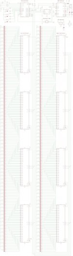
Another consequence of going for 60mm × 60mm unit dimensions is the redesign of the motorized fader modules with LED bargraphs. The off-the-shelf component I was planning to use will not fit, and it was not capable of showing different colors for the same LED anyway. With that in mind, I have decided to design my own 100mm 64-segment stereo bargraph, using the TLC5954 (Cf. attached schematic, or larger version from my original project). With a bit of luck, I should be able to fit 2 Bourns PSP motorized faders and 2 stereo bargraphs on a single 1 × 3 brick, which means that I could get 16 stereo channels with 16 faders by using only 4 grid modules, which is half the total width of my planned setup, leaving enough room for the keyboard and trackpad on the other half. Managing to cram all that goodness across less than a meter (960mm) was a huge driver in the decision to go for 60mm long bricks...
This is due to the fact that single-unit bricks require 8 screws: 4 for the cover and 4 for secure mounting on the underlying grid's PCB. As a result, they need thick 5mm walls for the through-holes or the blind threaded holes, which means that whatever the outside length is, the inside length is 10mm shorter.
With 42mm long bricks, the outer surface is 1,764mm², but the inner surface is only 1,024mm², which leads to a 58% surface efficiency ratio. But with 60mm long bricks, this ratio gets close to 70%, which is a lot better. And with multi-unit bricks, this ratio gets a lot higher of course.
As a result, I can easily get some "high-density" bricks like a 4 × 4 matrix of 16 × 3.5mm ports. This in turns provides much more flexibility when designing multi-control bricks that can be used in a versatile way. This can be seen on the new set of bricks required to clone all the Mutable Instrument modules. These clones could be designed with half as many different bricks (SKUs) as what was done for the 42mm × 42mm version.
These new dimensions also make it easier to include the Apple Magic Keyboard and the Apple Magic Trackpad 2, leading to the following setup.
Last but not least, these new dimensions now make it possible to mount the industrial version of the 3Dconnexion SpaceMouse and the newly-released Grayhill Touch Encoder on 1 × 1 bricks.
The only components that do not really fit are the Monome Grid and the LUMI keyboard, but I will build my own 128-pad grid module, and a micro piano keyboard is not really useful when a well-designed grid is available. For the grid control itself, I am getting a lot of inspiration from the excellent LinnStrument designed by Roger Linn.
Now, here comes the best part of the new design: I figured out a way to properly send signature signals over CV ports. Eurorack synthesizer modules use mono 3.5mm jacks for CV ports, but I could use stereo versions while remaining backward compatible. What that means is that outside audio and CV inputs produced by external components could still use mono jacks, while internal patching would be done using stereo jacks. For CV inputs and outputs, the CV signal would be sent on one channel, while its identifier (its signature) would be sent on another.
I also decided to remove many buttons from my standard Eurobrick modules, and to use 3.5mm ports instead. This is due to the fact that a 3.5mm port can be turned into a button by using a Klick Quick button dust plug. And the same can be done for turning a 3.5mm port into an LED. Doing so will dramatically reduce the number of bricks that will be needed for emulating a wide range of instruments.
Because I want to bridge the analog and digital domains, all the controls must be soft controls, which means using rotary encoders instead of potentiometers for example. Obviously, this creates some significant user experience (UX) issues. Some of these can be addressed by using motorized controls such as motorized faders, but this strategy cannot really be used for rotary controls, because motorized potentiometers are large (about 25mm in both length and width) and slow (about 12s to rotate 300°). As a point of comparison, a Bourns PSP motorized fader is just 14mm wide and can run its full 100mm travel distance within half a second.
Some rotary encoders used to be available with 24 or 32-segment LED rings, but these tend to be very large and are usually supplied by rather unreliable sources (none of the large suppliers like Bourns or Grayhill make them). Therefore, position feedback will have to be provided through the 5" touchscreen mounted on top of the single-board-computer.
For many applications, this is totally acceptable, but for some others, this design will break an important UX principle of proximity. Therefore, I have decided to add 6 rotary encoders underneath each and every single-board-computer, as can be seen on the latest setup. And for this setup, I have also decided to create a fairly advanced 1 × 1 brick made of a ED191AM8M 536 × 240 1.91" AMOLED display, 4 encoders, and 4 × 3.5mm ports (assuming that I can find small-enough encoders with push switch/detent). This brick (reference DE4P4) is currently used by 8 modules and will use the built-in display to provide visual position feedback for all 4 encoders located just underneath.
Another strategy is to use the Grayhill Touch Encoder, but this one is large and expensive, therefore will be used for applications where the rotary encoder is used for selecting an item from a list rather than setting a particular level for a numerical variable. For example, we will use it as a replacement for the algorithm selection wheel of the Mutable Instrument Warps module. I wish I could build a smaller alternative myself, but the smallest round OLED/AMOLED displays I could find have a 1.2" diameter, which makes it impossible to have 2 encoders side-by-side on a 60mm brick.
Another consequence of going for 60mm × 60mm unit dimensions is the redesign of the motorized fader modules with LED bargraphs. The off-the-shelf component I was planning to use will not fit, and it was not capable of showing different colors for the same LED anyway. With that in mind, I have decided to design my own 100mm 64-segment stereo bargraph, using the TLC5954 (Cf. attached schematic, or larger version from my original project). With a bit of luck, I should be able to fit 2 Bourns PSP motorized faders and 2 stereo bargraphs on a single 1 × 3 brick, which means that I could get 16 stereo channels with 16 faders by using only 4 grid modules, which is half the total width of my planned setup, leaving enough room for the keyboard and trackpad on the other half. Managing to cram all that goodness across less than a meter (960mm) was a huge driver in the decision to go for 60mm long bricks...
Attachments
Last edited:
- Status
- This old topic is closed. If you want to reopen this topic, contact a moderator using the "Report Post" button.
- Home
- Source & Line
- Digital Line Level
- 8 × AK5578EN + 8 × AK4499EQ ADC/DAC Boards