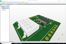
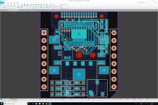
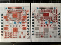
More Renderings
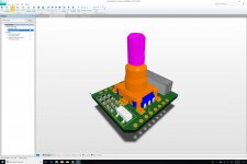
Here are a couple more renderings.
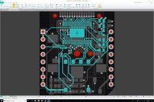
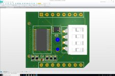
The first one shows the jumper switch used to turn the brick on and off while selecting the voltage level (+5V or +3.3V). To the left of that switch, we have the 12 discrete components used for debouncing the rotary encoder. And on the back we have the Hirose connector for mounting the mezzanine board with its 24 LEDs.
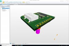
The second one shows the tri-state DIP switches used to set the brick's I²C address. This is something that will be done once when installing the brick on a plate (a plate can host 9 bricks). Therefore, it's not a problem to have it on the bottom side. That being said, the on/off switch available on the top side won't be exposed to the user either, because it will be blocked by the mezzanine board, which will also serve as top cover for the brick.
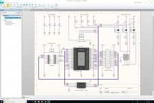
I have also attached an updated schematic, which shows that we have removed the power LED. This is due to the fact that it won't be visible when the mezzanine board is installed, therefore it serves no purpose other than debugging, and it was taking too much space in the wrong place on the board. Instead, removing it will allow us to mount some bolts and spacers that could be used to secure the mezzanine board on top of the base board, sandwiching the flange of the brick's frame.
Overall, I must say that I am very impressed by Altium CircuitStudio. This is a very powerful tool, and I have only scratched the surface. Past the first 10 to 20 hours of discovery, the tool feels really easy to use, and very stable. Unlike Eagle, it's a real joy to use, especially with a high quality monitor.
Here are a couple more renderings.
The first one shows the jumper switch used to turn the brick on and off while selecting the voltage level (+5V or +3.3V). To the left of that switch, we have the 12 discrete components used for debouncing the rotary encoder. And on the back we have the Hirose connector for mounting the mezzanine board with its 24 LEDs.
The second one shows the tri-state DIP switches used to set the brick's I²C address. This is something that will be done once when installing the brick on a plate (a plate can host 9 bricks). Therefore, it's not a problem to have it on the bottom side. That being said, the on/off switch available on the top side won't be exposed to the user either, because it will be blocked by the mezzanine board, which will also serve as top cover for the brick.
I have also attached an updated schematic, which shows that we have removed the power LED. This is due to the fact that it won't be visible when the mezzanine board is installed, therefore it serves no purpose other than debugging, and it was taking too much space in the wrong place on the board. Instead, removing it will allow us to mount some bolts and spacers that could be used to secure the mezzanine board on top of the base board, sandwiching the flange of the brick's frame.
Overall, I must say that I am very impressed by Altium CircuitStudio. This is a very powerful tool, and I have only scratched the surface. Past the first 10 to 20 hours of discovery, the tool feels really easy to use, and very stable. Unlike Eagle, it's a real joy to use, especially with a high quality monitor.
Attachments
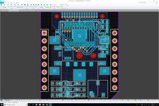
Cleaner Layout
Here is a much cleaner layout for the pull-up resistors connected to the LED driver. Since we're dealing with low-frequency digital signals, we do not need to reduce the lengths of traces to the absolute minimum, therefore we can be a bit more liberal with our placements, and take some board aesthetic considerations into account. This is not something that we'll be able to afford with the ADC and DAC board though...
Here is a much cleaner layout for the pull-up resistors connected to the LED driver. Since we're dealing with low-frequency digital signals, we do not need to reduce the lengths of traces to the absolute minimum, therefore we can be a bit more liberal with our placements, and take some board aesthetic considerations into account. This is not something that we'll be able to afford with the ADC and DAC board though...
Attachments
PCB Manufacturer Capabilities
I have verified that our design does not exceed the capabilities of JLCPCB. For example, I will use vias with a diameter of 20mil and a hole diameter of 10mil.
I have verified that our design does not exceed the capabilities of JLCPCB. For example, I will use vias with a diameter of 20mil and a hole diameter of 10mil.
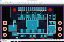
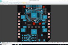
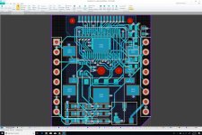
LED Signals Routing
We've managed to route the LED signals with a handful of vias. Now, we need to figure out how to route the debouncing circuit and the I²C address selector. After that, we'll add the power and ground layers. This is a lot more work than I was expecting though, and I sure am glad that we started with a tiny board before tackling the much more complex DAC board...
We've managed to route the LED signals with a handful of vias. Now, we need to figure out how to route the debouncing circuit and the I²C address selector. After that, we'll add the power and ground layers. This is a lot more work than I was expecting though, and I sure am glad that we started with a tiny board before tackling the much more complex DAC board...
Attachments
Last edited:
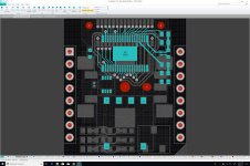
Wider Traces
All the 5mil traces have been thickened to 7.5mil, even though JLCPCB supports traces as thin as 3.5mil. Nevertheless, it's probably good practice to get traces as thick as they can be. The north part of the bottom layer for LED18..23 wasn't easy, but we found a way to make it work by lowering the Snap Grid level from 5mil down to 2.5mil.
All the 5mil traces have been thickened to 7.5mil, even though JLCPCB supports traces as thin as 3.5mil. Nevertheless, it's probably good practice to get traces as thick as they can be. The north part of the bottom layer for LED18..23 wasn't easy, but we found a way to make it work by lowering the Snap Grid level from 5mil down to 2.5mil.
Attachments

Cleaner Reset Trace
Here is an updated version (Before and After) with a much cleaner reset trace.
This is quite a lot of fun actually...
Here is an updated version (Before and After) with a much cleaner reset trace.
This is quite a lot of fun actually...
Attachments

Last edited:
Hole Tenting at Bottom
It's probably a good idea to tent the holes for the mikroBUS headers on the bottom side where they will be mounted. Of course, we need to keep the copper pads exposed on the top of the PCB where the headers will be soldered.
There are so many little details like that to take into account that PCB design is totally overwhelming at first, because everything comes at you all at once, and not much of it makes any sense initially. For example, I used to be totally lost with all the logical and physical layers defined by the EDA tool (be it Eagle, KiCad, or Altium). But now that I have a first board about halfway done, it's all starting to make sense, and I'm not intimidated anymore. This is a pretty darn good feeling actually...
Attachments
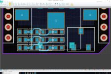
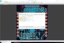
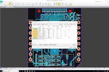
Layer Stack
We're almost there! We now have two internal planes, one for VCC and one for GND. The only thing that remains is +3.3V, which would be really hard to route on the top or bottom planes. Therefore, we have two options: either we split the VCC plane, or we add two additional layers, one for a +3.3V plane and one for something else. But looking at these stack-up options from Henry Ott Consultants, I cannot find one that matches our requirements. Any recommendation?
We're almost there! We now have two internal planes, one for VCC and one for GND. The only thing that remains is +3.3V, which would be really hard to route on the top or bottom planes. Therefore, we have two options: either we split the VCC plane, or we add two additional layers, one for a +3.3V plane and one for something else. But looking at these stack-up options from Henry Ott Consultants, I cannot find one that matches our requirements. Any recommendation?
Attachments
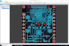
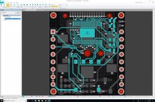
6-Layer Board
Here is the complete design with 6 layers, using JLCPCB's 6-Layer Impedance Control Stackup. Now that I understand a bit better how layers are working, we will probably design our DAC board with 6 layers in order to be able to use JLCPCB's services.
Tomorrow, we'll complete the board by adding markings. Then, we'll design the mezzanine board, which should be a walk in the park in comparison to its base board.
Attachments

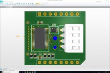
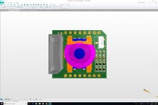
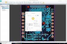
More on Overlay Markings
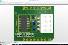
I am currently working on overlay markings, and I am starting to realize that we need to be pragmatic there. According to JLCPCB's capabilities, the minimum character width is 6 mil and the minimum height is 32 mil. I suspect that minimum width is more critical that minimum height, and the attached rendering shows characters in 6mil/30mil. This is pretty much as small as they will get. Therefore, we won't add markings to components, because they would be too small, or they would have to be positioned pretty far from the components themselves (for example for the 12 discrete components of the debouncing circuit on the South-West side of the top layer). This should not be a problem though, for we will provide detailed schematics and PCB layouts for all our products (this is the beauty of going Open Source).
As far as component outlines are concerned, we've also decided to remove them. Since the board will be assembled in a fab with surface-mounted components, there is no need for them, and they make the board a lot harder to read on the CAD tool. Instead, we're just using courtyards to make sure that our placements are in line with all datasheet recommendations.
What we will keep are the outlines for the two mikroBUS headers (because these will help with alignment for the manual soldering of headers), and some markings related to user settings, such as voltage level and I²C address. We will also add the name of the board and our logo, but we won't make any reference to the mikroBUS standard, because we're starting to deviate too much from it. First, we won't display the required pin markings. Second, we will most likely remove the notch at the South-East corner of the board in order to make room for a blind hole that will be used to attach the base board to the mezzanine board with four bolts. Bottomline: we'll be mikroBUS compatible at the electrical and interconnect levels, but not at the mechanical and visual levels. That being said, I doubt that any mikroBUS-compatible device will prevent the use of any of our bricks just because they're missing the little notch.
Attachments
Last edited:
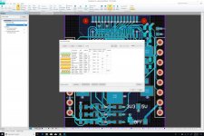
Question about multiple ground planes
We now have two ground planes (layers 2/6 and 5/6). My question is this: how do we decide which via should end on the top ground layer (2/6) and which should end on the bottom ground layer (5/6). Right now, all vias attached to the GND net end on the top ground layer (2/6). What are the best practices there? Or did I miss something altogether?
We now have two ground planes (layers 2/6 and 5/6). My question is this: how do we decide which via should end on the top ground layer (2/6) and which should end on the bottom ground layer (5/6). Right now, all vias attached to the GND net end on the top ground layer (2/6). What are the best practices there? Or did I miss something altogether?
Attachments
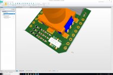
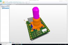
Screw Holes
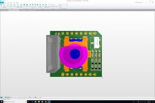
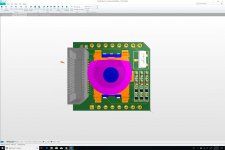
Here is what the base board looks like without any mikroBUS notch but with four through holes that could be used to secure the mezzanine board to the base board, using four M1.4 screws. These are the smallest screws with socket heads that can be found today (Cf. MetricScrews.us). Fortunately, they are available in a wide range of lengths (8mm, 10mm, 12mm, 16mm), and depending on the height of the four matching threaded inserts that we will mount at the bottom of the mezzanine board, we will probably use the 12mm or 16mm version.
The rendering does not do a great job of conveying how small the board actually is. At 1125mil × 1000mil (28.6mm × 25.4 mm), we really don't have much space to play with. In fact, for these screws, because of the two mikroBUS headers, we're limited to a 100mil × 100mil area (2.54mm × 2.54mm). In other words, the space occupied by a single 2.54mm header!
That being said, this type of subminiature hardware should be part of the fun when assembling the bricks. A bit like fixing a mechanical watch. And it reminds me of the hardware that I used to find when disassembling pocket electronic games in the early 80's (Cf. Octopus).
Attachments
Here is what the base board looks like without any mikroBUS notch but with four through holes that could be used to secure the mezzanine board to the base board, using four M1.4 screws. These are the smallest screws with socket heads that can be found today (Cf. MetricScrews.us). Fortunately, they are available in a wide range of lengths (8mm, 10mm, 12mm, 16mm), and depending on the height of the four matching threaded inserts that we will mount at the bottom of the mezzanine board, we will probably use the 12mm or 16mm version.
The rendering does not do a great job of conveying how small the board actually is. At 1125mil × 1000mil (28.6mm × 25.4 mm), we really don't have much space to play with. In fact, for these screws, because of the two mikroBUS headers, we're limited to a 100mil × 100mil area (2.54mm × 2.54mm). In other words, the space occupied by a single 2.54mm header!
That being said, this type of subminiature hardware should be part of the fun when assembling the bricks. A bit like fixing a mechanical watch. And it reminds me of the hardware that I used to find when disassembling pocket electronic games in the early 80's (Cf. Octopus).
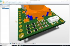
The diameter of a DIN 912 M1.4 screw's head is 2.6mm, which is 60 microns more than the 2.54mm area that we have to our disposal. Therefore, we've offset the four holes 5mil horizontally and vertically toward the center in order to keep the screw heads within the board's footprint. This offset is not a problem, because the screw heads will be on the top side, while the mikroBUS headers will be on the bottom side, therefore they won't interfere with each other.
These screws aren't super common, so it can be hard to find their dimensions. Here is the M1.4 × 10 version.
Now we need to find matching mounting hardware for the mezzanine board. This might be a bit of a challenge...
Attachments
We now have two ground planes (layers 2/6 and 5/6). My question is this: how do we decide which via should end on the top ground layer (2/6) and which should end on the bottom ground layer (5/6). Right now, all vias attached to the GND net end on the top ground layer (2/6). What are the best practices there? Or did I miss something altogether?
All of your vias should be through the entire board, unless you are intentionally using blind or buried vias. The two ground planes will be tied together when all GND vias go through both planes. You can add extra via stitching later once you're done also.
All of your vias should be through the entire board, unless you are intentionally using blind or buried vias. The two ground planes will be tied together when all GND vias go through both planes. You can add extra via stitching later once you're done also.
Chris,
Thanks a lot for the clarification. That's what I did at first, but it somehow kept the connections lines (the thin yellow lines) when I did that. I will try again.
Chris,
Thanks a lot for the clarification. That's what I did at first, but it somehow kept the connections lines (the thin yellow lines) when I did that. I will try again.
I found the problem: I had actually missed three vias. Problem fixed, and all vias start from the top and end at the bottom.
Thanks!
Attachments
- Status
- This old topic is closed. If you want to reopen this topic, contact a moderator using the "Report Post" button.
- Home
- Source & Line
- Digital Line Level
- 8 × AK5578EN + 8 × AK4499EQ ADC/DAC Boards