Footprint for Rotary Encoder
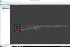
Here is the footprint for the rotary encoder, based on this datasheet. Because of limitations with Altium CircuitStudio, we cannot drill rectangular through holes. As a result, we made them rounded slots. This should work fine, but we should test that with a bare PCB, just to make sure. Also, this screenshot shows how holes #4 and #5 are joined together to make an oblong through hole, exactly as described in the specification.
Here is the footprint for the rotary encoder, based on this datasheet. Because of limitations with Altium CircuitStudio, we cannot drill rectangular through holes. As a result, we made them rounded slots. This should work fine, but we should test that with a bare PCB, just to make sure. Also, this screenshot shows how holes #4 and #5 are joined together to make an oblong through hole, exactly as described in the specification.
Attachments
Here is the footprint for the rotary encoder, based on this datasheet. Because of limitations with Altium CircuitStudio, we cannot drill rectangular through holes. As a result, we made them rounded slots. This should work fine, but we should test that with a bare PCB, just to make sure. Also, this screenshot shows how holes #4 and #5 are joined together to make an oblong through hole, exactly as described in the specification.
Well, this did not make much sense actually: if we can drill slots for #1 and #2, we should be able to drill #4 as a single slot as well, instead of drilling two holes so close to each other, which would probably result in a really poor finish. This latest revision is much better.
Unfortunately, there is no CAD model for the K model of the EC11Series... But since this component won't need to be assembled at the factory, this is probably fine. We just asked Alps' sales department for one, just in case, but my hopes a really low on that one...
Attachments
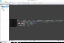
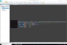
Cleaner Schematic
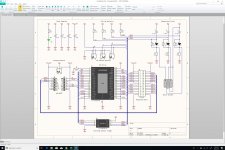
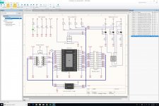
Here is an updated version of the schematic for the E1 base board. The circuit around the rotary encoder is cleaner, and labels have been added to the schematic's main section. Overall, I like this layout a lot better than the original, especially with respect to the debouncing circuit, which did not outline the clear pattern that we see clearly repeated three times at the top right of the latest design. The I²C Address Selector is also much better separated from the four pull-up resistors, and while our design is a bit denser, it makes a much better use of the space available, therefore is quite a bit easier to read.
But what's most interesting to me with this exercise is the increased level of familiarity with the overall circuit that such a piece of work leads to. No matter how many times I read the documentation for the Knob G Click, I kept overlooking some parts, either because I did not deem them important, or because I did not understand them fully.
A great example of this is the set of three jumpers that are used to set the I²C address. Quite frankly, I put them on the schematic without having any understanding of their function. Of course, this was pure laziness on my part, but there are so many things to take into consideration when designing such a system that priorities have to be established, and this one did not rank very high at first.
As it turns out, I was wrong, and now that I understand what these jumpers are for, I realize that there is some room for improvement. Instead of using jumpers that have to be soldered, we could use DIP switches. But these jumpers offer three states : 1 connected to 2, 2 connected to 3, and no connection at all. Fortunately, we can use a 4-position 3-state DIP switch like the TIM-04-V-T/R. I did not know these existed until I saw them on the Fusion board, and they are awesome. These switches come with 4, 5, 8, 9, and 10 positions, and the 4-position model will be perfect for us, because we'll be able to use the fourth one for the voltage selector, which will have three options:
- +3.3V
- Off
- +5V
These changes should make the brick a lot more user friendly...
Another lesson learned is that deep familiarity with the full range of components currently available can make a huge difference in a design. This must be obvious to any electrical engineer, but for a software person like myself, the approach is usually different: while we use many libraries to build a new piece of software, the range of options is much more limited. Therefore, I really need to change my way of thinking if I want to improve my design skills.
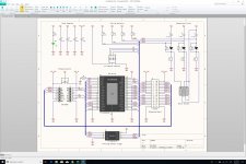
Attachments
Last edited:
Fortunately, we can use a 4-position 3-state DIP switch like the TIM-04-V-T/R.
The TDS04SGNNTU04 is probably a more mainstream alternative.
The TDS04SGNNTU04 is probably a more mainstream alternative.
But I got it wrong: we cannot use a single 4-position DIP switch, because the + and - references are different for the I²C address selector (VCC and GND) and for the voltage selector (+5V and +3.3V).
Oh well, we can still use it for the I²C address selector I guess...

Voltage Selector
Here is an updated schematic with the TDD01H0SB1R jumper switch for the voltage selector. As a result, we do not have any soldered jumpers anymore, which is a really good thing. Of course, this will increase the cost of our BOM by $2 to $3, but our target audience does not know how to use a soldering iron anyway...
This voltage selector is probably overkill on this brick, because we will always have both +5V and 3.3V available through our mikroBUS port, but it's a good exercise to play with this type of component and gather some experience with it.
And just to be clear, we're fine using these DIP switches because the E1 brick does not carry any sensitive signal. This kind of arrangement for analog signals or high-speed digital signals is totally out of the question on the upcoming DAC block.
Attachments

Last edited:
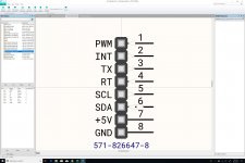
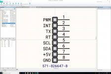
Reference Designators
For all our reference designators, we are using this standard table, and we're adding a few more that are missing, like E for encoders.
For all our reference designators, we are using this standard table, and we're adding a few more that are missing, like E for encoders.
Attachments
Passive Pins
We've turned all the pins of our mikroBUS headers as passive pins in order to make sure that unconnected pins do not violate any default rules. This is motivated by the fact that most pins on these headers are optional.
We've turned all the pins of our mikroBUS headers as passive pins in order to make sure that unconnected pins do not violate any default rules. This is motivated by the fact that most pins on these headers are optional.
Attachments
Compilation
The schematic was successfully compiled with no errors. We just have warnings regarding nets with no driving source (because of the fact that we made all the mikroBUS pins passive) and buses with unconnected lines (these are acceptable as far as I can tell). Time to place all our components on the PCB...
The schematic was successfully compiled with no errors. We just have warnings regarding nets with no driving source (because of the fact that we made all the mikroBUS pins passive) and buses with unconnected lines (these are acceptable as far as I can tell). Time to place all our components on the PCB...
Attachments
Base Board PCB
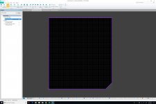
Here is the PCB for the base board: 1125mil × 1000mil, with a notch at the bottom right, per mikroBUS specification. Technically, the board only needs 2 layers, but we might make it a 4-layer design in order to gain experience with this stacking strategy.
Here is the PCB for the base board: 1125mil × 1000mil, with a notch at the bottom right, per mikroBUS specification. Technically, the board only needs 2 layers, but we might make it a 4-layer design in order to gain experience with this stacking strategy.
Attachments
Top Layer
Here is what the top layer looks like with the mikroBUS headers, the Hirose connector for the mezzanine board, and the surface-mounted encoder. It's a tight fit, but it should work. One thing should be noted though: the rotary encoder won't be vertically centered on the brick, because of the Hirose connector at the bottom. Instead, it will be offset by just under a quarter inch upward. This should not be a problem though. We could reduce that offset by rotating the encoder by 90 degrees, but it would prevent us for displaying the markings for the mikroBUS pins, and the encoder would still not be centered on the base board. That being said, we might be able to center it in relation to the mezzanine board, therefore in relation to the brick itself. We'll try that out just to make sure...
Note: don't pay attention to the net names, for they're probably incorrect. We're going to work on that later once the mechanical layout has been figured out.
Attachments
Last edited:
 (because my daughter asked for it)
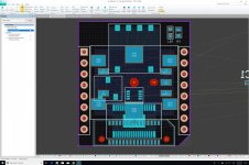
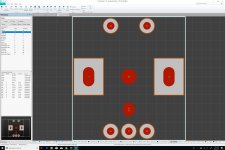
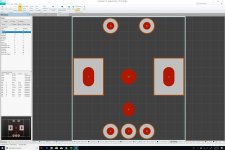
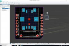
First Component Placement
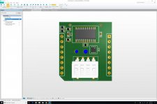
Here is the base board with all components placed. They take pretty much the entire space on both side of the PCB, at the exception of the four corners, which might be used for surface-mounted bolts. While it might be possible to do the routing through two layers only, we will probably do it with four layers, just to learn a bit more about the process.
Here is the base board with all components placed. They take pretty much the entire space on both side of the PCB, at the exception of the four corners, which might be used for surface-mounted bolts. While it might be possible to do the routing through two layers only, we will probably do it with four layers, just to learn a bit more about the process.
Attachments
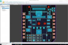
Here is the base board with all components placed. They take pretty much the entire space on both side of the PCB, at the exception of the four corners, which might be used for surface-mounted bolts. While it might be possible to do the routing through two layers only, we will probably do it with four layers, just to learn a bit more about the process.
Also, we've managed to perfectly perfectly center the encoder on the board, which is quite nice.
Also, we've managed to perfectly perfectly center the encoder on the board, which is quite nice.
Will the encoder knob block visual access to the LEDs at all?
Will the encoder knob block visual access to the LEDs at all?
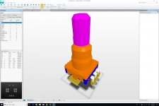
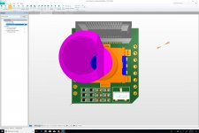
Here are some 3D rendering that should help understand the stack. The first picture shows the top of the board, while the second one shows the bottom. The Hirose connector on the north side of the board's top is used to plug a mezzanine board on which the 24 LEDs will be mounted. This mezzanine board will have a 10mm round through hole in its center in order to let the encoder's shaft through. These LEDs will be as far away as the center as possible in order to remain visible even when a 20mm diameter knob is being used.
Does that make sense?
Attachments
- Status
- This old topic is closed. If you want to reopen this topic, contact a moderator using the "Report Post" button.
- Home
- Source & Line
- Digital Line Level
- 8 × AK5578EN + 8 × AK4499EQ ADC/DAC Boards