LED Mezzanine Board
The E1 brick with a single encoder and a 24-LED ring will be made of a base board and a mezzanine board, the former populated with the LED driver, and the latter with the LEDs. But one question remains: how can we make a cover for this complex brick that will let the LEDs' light through?
While pondering this question, an idea came to mind: how about using the mezzanine board itself as the cover? This could be achieved by mounting all the components on one side of the board (24 LEDs and 2 Hirose connectors), while taking advantage of the fact that a PCB's substrate is usually translucent, hence could be used as light guide.
Of course this design would not be without its challenges. First among them is the fact that the LEDs would now point downward. Therefore, we would need some kind of reflective surface in order to bounce their light back up. Second, if we were to use a 4-layer PCB for the mezzanine board, we would probably want to keep some traces on the two middle layers with a star pattern in order to compartmentalize our 24 light sources (we don't want the light to diffuse throughout the board). And we would want to make sure that the solder mask applied to the backside of the board (the one directly exposed to the user) would have the right texture (the MikroE Fusion board has a really nice black satin finish).
This might be a bit crazy, but if we manage to get the light through, all the user would see from the top is a continuous arc of light shining through a black brick's cover, and it would spare us the cost of developing a separate cover. Furthermore, we could probably use this technique for many other bricks.
And one option could be to use reverse-mount LEDs, assuming that we could find some that are small enough.
And one option could be to use reverse-mount LEDs, assuming that we could find some that are small enough.
Here we go: VLDB1232R-08
This is really cool, because all we need is a round through hole in the PCB for each of the 24 LEDs. Most importantly, if we manage to use this technique for all the other bricks, it will let us benefit from the existing PCB supply chain in order to manufacture a lot of our mechanical components, with exceptional precision and very low costs.
To do so, we should find board-to-board connectors that are cheap enough, because we would need four of them for every brick, and some bricks might use them for nothing more than the mechanical interconnect, leaving all pins floating on both sides. This Hirose connector is a good example. At $0.50 a piece, it would add "only" $2 to a brick's BOM. It's not an insignificant amount, but machining custom covers or doing injection moulding would be expensive as well, especially when doing small production runs.
This is a really promising avenue...
Last edited:
Here we go: VLDB1232R-08
Here is an even better options (smaller): XZFBB45S-9
And with that kind of approach, we do not even need any hole to be drilled in the PCB. Instead, we would just leave the PCB bare without any copper nor solder mask on the areas where holes would have to be drilled. This should be enough to let the right amount of light through, especially if we use the high-intensity version of this reverse-mount LED.
Brick Mechanical Design
If all bricks were designed with two PCBs, the stack of PCBs could actually provide the mechanical interconnect with the brick's frame, which could be made from a simple aluminum square profile on which an internal flange would have been machined. In essence, the two PCBs would mount on each side of the flange, making a sandwich out of it. And if we were to remove the notch at the bottom right corner of the base board (as specified in the mikroBUS specification), we would have enough room for adding 4 screws that could be used to secure the whole assembly:
1. Mezzanine Board
2. Frame (via flange)
3. Base Board
This is really interesting, because it would solve a ton of mechanical problems with a very simple and low-cost design, while providing a very clean look for the finished product.
ER8 Series
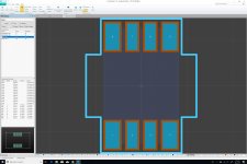
For our board-to-board connectivity, we need pairs of connectors that will give us enough vertical clearance for components like the EC11J1524413. The datasheet shows that we need at least 4.5mm if we want our mezzanine board to stand on top of the encoder's base, with a simple 10mm round through hole. Unfortunately, the mating height of many Hirose mezzanine connectors is 4.3mm or less. Therefore, we need to use a special series called ER8, which provides multiple stacking heights, from 7mm to 12mm. In our case, we'll be satisfied with 7mm (we're trying to keep things as low profile as possible). And with this form factor, we could have 30 pins on an 18mm-long connector, which would fit perfectly between out two mikroBUS connectors. And with that many pins, we would just need a single pair of connectors (one plug and one receptacle) for our 24 LEDs.
For our board-to-board connectivity, we need pairs of connectors that will give us enough vertical clearance for components like the EC11J1524413. The datasheet shows that we need at least 4.5mm if we want our mezzanine board to stand on top of the encoder's base, with a simple 10mm round through hole. Unfortunately, the mating height of many Hirose mezzanine connectors is 4.3mm or less. Therefore, we need to use a special series called ER8, which provides multiple stacking heights, from 7mm to 12mm. In our case, we'll be satisfied with 7mm (we're trying to keep things as low profile as possible). And with this form factor, we could have 30 pins on an 18mm-long connector, which would fit perfectly between out two mikroBUS connectors. And with that many pins, we would just need a single pair of connectors (one plug and one receptacle) for our 24 LEDs.
Last edited:
Port Connector
With our dual PCB brick design, we should use the 161-MJ355W-EX TRS connector for our Audio/CV ports. It needs 10.2mm of vertical clearance, which means that by using the right Hirose ER8 connectors with 10mm matting height, we can actually use it as vertical spacer, which needs to be 10.05mm ±0.05mm (this is almost too good to be true). With this connector, we won't have any problem fitting 4 within a brick. And by adding reverse-mounted LEDs on the mezzanine PCB, we should be able to add 6 LEDs to every port, indicating whether it carries an audio signal, a CV signal, or a clock/gate, either as input (blue) or as output (green). And we should be able to add some silkscreen markings to make all this crystal clear to the end user.
I'm starting to really like this design...
Another benefit of using a PCB as brick cover is that we will be able to add silkscreen markings on them, at virtually no additional cost.
Don't forget that you need good shielding so that your system doesn't pickup electro-magnetic-field energy nor radiates it.
Don't forget that you need good shielding so that your system doesn't pickup electro-magnetic-field energy nor radiates it.
Right. Can I do that with middle-layer pours on the mezzanine boards used as brick covers?
Following the different pieces of advice that I received from sciencesky and chris719, I have updated the footprints for SOT765-1 and SOT1331-1. setting proper values for the Paste Mask Expansions and Solder Mask Expansions. And by using a large value for the former on SOT1331-1, I managed to fully expose the die pad, then add the 24 segmented paste pads.
For both footprints, I also made sure to include the boundaries for the occupied areas on the "Courtyard Top" layer. For these, I set a width of 0.1mm, but I don't think it matters, since it won't be printed anywhere. Instead, it's just used as a way to make sure that components are not placed too close to each other on the PCB.
Many thanks to sciencesky and chris719 for their help! I've learned a lot in the process.
And I sure am glad to go through all this for a seemingly trivial project like an encoder with LED ring, because making mistakes for it will be a lot less painful than making mistakes for the AK4499EQ-powered DAC board.. Learning to walk before we run...
The SOT765-1 footprint could be better.
The solder mask isolation between your pads is too small!
It looks like the solder mask opening on each side of the pad is bigger than the actual remaining solder mask between two pads.
As said before you can make all pads 0.3mm wide, solder mask expansion -> 0.05mm, solder paste expansion -> -0.05mm.
For the other part you can place VIAs in the center pad now or later in the design.
Don't forget the Top Overlay aka Silkscreen and also a placement outline which is Mechanical Layer 15 in Altium Designer.
It is good practice to place the placement outline 0.3mm away from the copper pads.
With our dual PCB brick design, we should use the...TRS connector for our Audio/CV ports.
Sure you don't want connectors with some switching function(s) that can be used to detect mating connector insertion?
Right. Can I do that with middle-layer pours on the mezzanine boards used as brick covers?
Don't know that. But it needs to be a very low impedance connection to chassis ground.
I lost the overview over your design

The SOT765-1 footprint could be better.
The solder mask isolation between your pads is too small!
It looks like the solder mask opening on each side of the pad is bigger than the actual remaining solder mask between two pads.
As said before you can make all pads 0.3mm wide, solder mask expansion -> 0.05mm, solder paste expansion -> -0.05mm.
For the other part you can place VIAs in the center pad now or later in the design.
Don't forget the Top Overlay aka Silkscreen and also a placement outline which is Mechanical Layer 15 in Altium Designer.
It is good practice to place the placement outline 0.3mm away from the copper pads.
Oh, I get it now! I had made the Paste Mask Expansion -0.05mm and the Solder Mask Expansion +0.075mm, thinking that it would be better than +0.05mm, but you're right, decreasing it to +0.05mm looks better. Here is an updated screenshot (Paste Mask Expansion: -0.05mm | Solder Mask Expansion +0.05mm). Please let me know if I got it right this time.
Yes, I will add vias to the SOT1331-1, but I still need to study them a bit more before adding them to the design (types, sizes, etc.).
As far as the placement outline is concerned, the Click Board is not using it for most of its components, and I'm not sure that we need it either, especially on such a small board. What's your take?
Attachments
Don't know that. But it needs to be a very low impedance connection to chassis ground.
I lost the overview over your design
No kidding... I have a hard time following the design myself...
More seriously, I'll try to make some 3D models of the whole stack (USB trays > USB plates > mikroBUS bricks), but I'm not sure I want to invest the time on Fusion360 (which I'm currently familiar with) or Solidworks (which I should probably learn once and for all).
So much to learn...
Sure you don't want connectors with some switching function(s) that can be used to detect mating connector insertion?
Well, I don't really have the choice of connectors if I want to remain backward compatible with existing Eurorack modules, and I really, really want that.
Therefore, the only deviation from mono 3.5mm audio jacks that I can afford is to use stereo phone jacks, or any 3.5mm jack for that matter (we're not really limited to 3 pins, even though I'm not sure what additional pins could bring). But I'm going to use the right channel to carry a digital signature for the signal, therefore I should be able to detect what signal is carried by the patch cable being plugged into the "universal" port.
From a user experience standpoint, I want to avoid asking the user to click on a button in order to switch the port's function. This function should be defined by the brick itself, by the plate hosting the brick (instruments will be implemented at the plate level usually, a plate being a host for 3 × 3 bricks), or by the software itself.
Last edited:
Encoder for E4 Brick
Following our latest brick design, we've checked every single brick to make sure that it could be built accordingly, and as far as we can tell, everything seems to be working fine. One brick that created some trouble is the E4 quad-encoder brick, because fitting 2 × 2 encoders on a single square inch is definitely a challenge (with any design by the way, we had simply overlooked this with our earlier designs, assuming that we could find the right encoder). After quite a bit of research, we finally found the CTS 291 series, which seems to fit the bill perfectly, especially when using the version without Schmitt trigger, without locating lug, and with .050” pitch pins facing rear. Its overall footprint is 14.35mm × 13.2mm, but what makes it really work for our design is that all six through-hole pins are on one side, leaving room for the Hirose connectors that are needed to connect the mezzanine board to the main board. All the other encoders we found were larger and had pins on all four sides, making it impossible to fit everything on our mezzanine board.
Following our latest brick design, we've checked every single brick to make sure that it could be built accordingly, and as far as we can tell, everything seems to be working fine. One brick that created some trouble is the E4 quad-encoder brick, because fitting 2 × 2 encoders on a single square inch is definitely a challenge (with any design by the way, we had simply overlooked this with our earlier designs, assuming that we could find the right encoder). After quite a bit of research, we finally found the CTS 291 series, which seems to fit the bill perfectly, especially when using the version without Schmitt trigger, without locating lug, and with .050” pitch pins facing rear. Its overall footprint is 14.35mm × 13.2mm, but what makes it really work for our design is that all six through-hole pins are on one side, leaving room for the Hirose connectors that are needed to connect the mezzanine board to the main board. All the other encoders we found were larger and had pins on all four sides, making it impossible to fit everything on our mezzanine board.
Blind Holes in PCB for Connector Indexing Pins
I just realized that the ER8 connector that I want to use has two indexing pins that require a hole to be drilled on the PCB on which it is mounted. These pins are 1.07mm tall. This is not a problem for the base board, but it is for the mezzanine board: it would be unsightly to have two holes there. This top PCB is likely to be 1.6mm to 2mm thick. My question is the following: is it possible for most PCB manufacturers to drill a blind hole? In that case, instead of having two through holes, we would have two blind holes that would be about 1.2mm deep.
I just realized that the ER8 connector that I want to use has two indexing pins that require a hole to be drilled on the PCB on which it is mounted. These pins are 1.07mm tall. This is not a problem for the base board, but it is for the mezzanine board: it would be unsightly to have two holes there. This top PCB is likely to be 1.6mm to 2mm thick. My question is the following: is it possible for most PCB manufacturers to drill a blind hole? In that case, instead of having two through holes, we would have two blind holes that would be about 1.2mm deep.
Last edited:
It can probably be done, but you won't be able to solder it properly since it's designed to be a through-hole.
I'd just pick a fully surface mount connector, there are probably some options out there.
I would much rather do that indeed, because blind holes in PCBs seem to be on the exotic side, therefore super expensive. But finding an SMD connector without any indexing pin and a fairly tall mating height is not super easy, especially because the mating height is not a standard parameter on the distributors' websites. I'll keep looking though.
- Status
- This old topic is closed. If you want to reopen this topic, contact a moderator using the "Report Post" button.
- Home
- Source & Line
- Digital Line Level
- 8 × AK5578EN + 8 × AK4499EQ ADC/DAC Boards