Hello diyaudio,
Let's say you had a DSP with a master clock. You have a TDM8 configuration (i2s). You have 4 DAC's on different PCB's and you need to feed that clock signal to all 4 DAC's over 6 inch ribbon cables. What's the right way to split up the master clock signal to each DAC separately while maintaining accuracy? Is there a particular master clock Repeater IC?
Jay
I'm starting to answer my own question.
I'll start looking at the freedsp boards for examples.
MCLK distribution
All main-boards and slave boards need to be synchronous to a common master clock (MCLK). Therefore future freeDSP main-boards must feature a MCLK distribution circuit, which provides several synchronous but independant MCLK outputs. These will supply a MCLK to the onboard DSP and also to each expansion board via the standard freeDSP expansion connector.
freeDSP main-boards provide MCLK: 24.576 MHz
freeDSPx expansions receive MCLK via standard freeDSP expansion connector
I'll start looking at the freedsp boards for examples.
If you want a basic clock buffer and distributor, you might look at NB3L553. If you want to regenerate a clock and produce output with very low jitter then LTC6952 is very sophisticated part. It can also be used, among other things, for synthesizing a new clock frequency at some a/b ratio relative to a reference clock, where 'a' and 'b' are integers. Not cheap though.
Hello Markw4,
Thanks! That's very helpful.
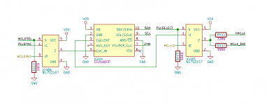
freeDSP-CLASSIC-SMD-B-master uses IDT2305NZ like this.

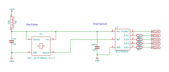
freeDSP-ALLinONE uses IDT2309NZ like this.

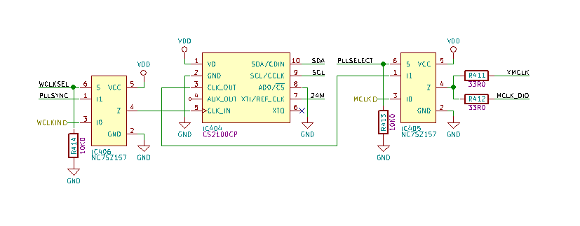
freeDSP-aurora seems to be using the NC7SZ157... Like this. Although the datasheet is very technical and I'm not positive what this is doing. In fact, I'm not sure that it's distributing the clock as much as just maybe strengthening it?
I'll probably just follow the lead from the freeDSP-CLASSIC-SMD-B for my project. Or I'll look into the NB3L553. Seems simple.
If you want a basic clock buffer and distributor, you might look at NB3L553. If you want to regenerate a clock and produce output with very low jitter then LTC6952 is very sophisticated part. It can also be used, among other things, for synthesizing a new clock frequency at some a/b ratio relative to a reference clock, where 'a' and 'b' are integers. Not cheap though.
Thanks! That's very helpful.
freeDSP-CLASSIC-SMD-B-master uses IDT2305NZ like this.
freeDSP-ALLinONE uses IDT2309NZ like this.
freeDSP-aurora seems to be using the NC7SZ157... Like this. Although the datasheet is very technical and I'm not positive what this is doing.
In fact, I'm not sure that it's distributing the clock as much as just maybe strengthening it?I'll probably just follow the lead from the freeDSP-CLASSIC-SMD-B for my project. Or I'll look into the NB3L553. Seems simple.
Attachments
It is providing multiple copies of the clock that can go to different parts of the circuitry. In that case, its often good to have low skew (the timing difference between the different clock copy outputs) and low jitter from various noise sources including power supply noise due to all the output channels switching at once, and whatever other noise may be on the power pins of the clock buffer.
Problems in your Kickstarter adventure?
Lol, I'm still eagerly waiting for the Aurora. But ultimately may redesign it without it's ADC/DAC parts so I can connect add-on boards instead. Or may possibly continue to research the Teensy Bridge I've been working on. So I might need to distribute some clocks!
I just realized something. I know when going from board to multiple boards it's a good idea to have clock distribution. But what about one board with multiple DAC/ADC parts. Is it ok to have 2 DAC's on one mclk source? 3 DAC's? I just realized that I might need clock distribution on each add-on board in addition to the main board because each add-on board will have multiple ADC/da parts. Any input is appreciated!
Transporting clock signals between boards without picking up a likely significant amount of jitter would seem to require some careful thought and engineering. Ribbon cables are not as good as more rigid connections. Use quality gold-flashed or gold plated connectors, use ground pins (and wires for any cables) adjacent to clock signals on both sides for improve signal integrity. Perhaps better to convert LVCMOS signals to LVDS or LVPECL for transport across multiple boards. The signals can be converted back to LVCMOS when and where needed. Otherwise, 'clock cleaner' chips and or techniques can be used to help clean up clock signals. When using additional chips such as LVDS <> LVCMOS converters and or clock cleaners/regenerators it might be good to look at the added jitter they may cause down at 10Hz offset. Many devices have impressive jitter numbers specified at 12kHz offset, which is meaningless for audio.
My current project is reversely similar to your's: Same clock domain, Multiple (4) I2S to a Single DAC Selector:Hello diyaudio,
Let's say you had a DSP with a master clock. You have a TDM8 configuration (i2s). You have 4 DAC's on different PCB's and you need to feed that clock signal to all 4 DAC's over 6 inch ribbon cables. What's the right way to split up the master clock signal to each DAC separately while maintaining accuracy? Is there a particular master clock Repeater IC?
Jay
- Amanero, XMOS, AK4118, RaspberrryPi (or BeagleBone) will be the isolated input
- Low jitter and phase noise I2C controlled oscillator will feed Si5317 (or Si5319) configured for 4 CMOS same frequency output, so one MCLK for every I2S source
- PO74G374A (4 pcs.) will be the source selector, but it will act also as the I2S signals re-aligner (by the rising edge of every MCLK)
- AK4137 will be the output
...Si5317...
Looking at Si5317 data sheet, page 34, phase noise already looks poor at 100Hz. They don't even bother to show it at 10Hz and 1Hz offsets.
Might be nice to be able to switch in a crystal clock, maybe one on a socket so different clocks could be compared. Iancanada offers clock mounting boards that can mate to a a wide dip socket (of good quality, preferably all gold contacts for lowest jitter). Highly recommended to try.
Good point, Mark, thank you for switching clocks idea.
I switched to Si5394 (still worse on 100Hz BW, but 50% better than 5317), I already ordered it.
I will use all its 4 clock inputs, so my reference I2S out board will also be able to select from 4 different oscillators - Crystek, NDK, etc, any format LVPECL, LVCMOS...
I also have decided about the four I2S sources:
- Amanero = USB 1
- AK4118 = COAX 1
- XU216 = USB 2 + COAX 2
- BeagleBone
Thorp,
Very interesting plan. Since you will have an Amanero, that makes high sample rate DSD with synchronous mode clocking possible. Very nice sound quality that way. Many people seem to like HQplayer software to upsample CD and other source material to DSD512. They say that gives the best SQ of the choices they have found. Maybe something I will be trying before too long.
Very interesting plan. Since you will have an Amanero, that makes high sample rate DSD with synchronous mode clocking possible. Very nice sound quality that way. Many people seem to like HQplayer software to upsample CD and other source material to DSD512. They say that gives the best SQ of the choices they have found. Maybe something I will be trying before too long.
After thinking more about what I'm trying to do, I wonder if CyberPit's method is the right way to do it. By adding a Digital Buffer to the I2S lines (including clock, and all other lines), I should be able to transmit/drive/receive a cleaner signal. Yes?
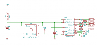
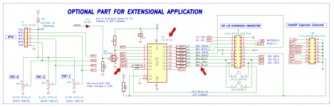
So I have the following schematic. What if I added an Octal Line Driver/Buffer to this circuit, so that each expansion port has a stronger signal. What do you think?
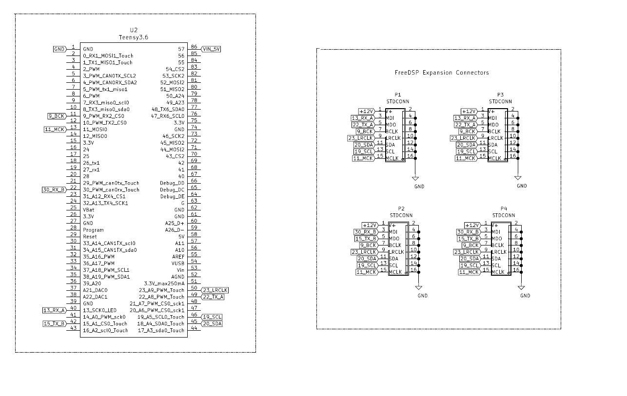
Here is what it will look like without any buffer.... But I'm planning a power supply, and I'm debating what driver I might need to ensure that the signal carries to all 4 ports, and over ~6 inches of IDE cable.

Basically the Teensy 3.6 has 2 I2S lines. The lines share the BCK, LRCLK, SDA, SCL, & MCK. Then there are two I2S RX and TX (receive and send) buses. The point of this project is to expose the two buses, so that pairs of DAC/ADC parts can be connected.
So I have the following schematic. What if I added an Octal Line Driver/Buffer to this circuit, so that each expansion port has a stronger signal. What do you think?
Here is what it will look like without any buffer.... But I'm planning a power supply, and I'm debating what driver I might need to ensure that the signal carries to all 4 ports, and over ~6 inches of IDE cable.
Basically the Teensy 3.6 has 2 I2S lines. The lines share the BCK, LRCLK, SDA, SCL, & MCK. Then there are two I2S RX and TX (receive and send) buses. The point of this project is to expose the two buses, so that pairs of DAC/ADC parts can be connected.
Attachments
- Status
- This old topic is closed. If you want to reopen this topic, contact a moderator using the "Report Post" button.
- Home
- Source & Line
- Digital Line Level
- Clock Repeater IC, Jitter correction ic, clock distibution