Hello, in reference to the following similar schemes:
1) 1. Jitter suppression and PLL design
2) http://www.audiocostruzioni.com/a_d/elettroniche/elettroniche-varie/dac-II-maurizio-daniele/PLL.jpg
can you please explain to me why the phase detector (two flip flops and a nand port) should work with a 1:16 frequency divider (11.289MHz / 16 = 705KHz) of the input frequency, instead of working just comparing the two entire input frequencies (MCK and VCXO, both at 11.2896MHz) ?
In simple words what happen if I would use 1:1 (no divider), or 1:2 or 1:4 or even 1:32 frequency dividers?
Attachments
You only need the frequency divider if you want the output clock to run faster than the input i.e. you want a frequency multiplier. If you run at 11.2896MHz input frequency and only want that frequency for output then you've no need for a divider.
That was what I thought too, but it is not the case: in the above examples both input and output frequencies are the same (11.2896), but the PLL works at 1:16
That's not how I read the first link - here are some quotes :
Later, when describing the filter that comes after the phase detector, we read :
For our design we chose to use the sample word buffer: Having the PLL in phase-lock on the word clock (44.1 kHz), does not require longer buffer queues. Operating the PLL on the input bit-clock (32 bits x 2 samples x44.1 kHz = 2.8224 MHz) would have been another usefull option but would leave a small phase (timing) margin for the very slow changing oscillator frequency........This allows easy cooperation with an external PLL locking on the word clock.
Later, when describing the filter that comes after the phase detector, we read :
As the actual input signal is a 705kHz digital signal with lots of higher harmonics, these AC components are significantly damped before reaching the opamp.
Sorry, but still not clear.
I cannot explain the use of U11 and U12 in the following:
http://members.chello.nl/~m.heijligers/DAChtml/dig_r2c.pdf
Do you?
I cannot explain the use of U11 and U12 in the following:
http://members.chello.nl/~m.heijligers/DAChtml/dig_r2c.pdf
Do you?
I cannot explain the use of U11 and U12 in the following:
http://members.chello.nl/~m.heijligers/DAChtml/dig_r2c.pdf
They're divide-by-16 counters so that the phase detector's working at 705.6kHz, not 11.2896MHz. Entirely consistent with the text where it says :
To return to my original comment (post #2) - the divider's present because their PLL is working at 705.6kHz, not at 11.2896MHz. Its a frequency multiplier.In our design the PLL operates on a 16x divided master clock frequency, or 11.289MHz / 16 = 705 kHz.
their PLL is working at 705.6kHz, not at 11.2896MHz. Its a frequency multiplier.
That is clear, thanks. Why in your opinion they choose to work at 705.6k and not at 11.2896M saving two chips? Why 705.6k and not at 1.4112M or 2.8224M or higher? More stability? More precision? Lower cut-off LPF?
From reading the link I got the impression the reason they run at a much lower frequency is the same one @MarcelvdG mentioned - they want to deal with the possibility of more than +/-44nS of jitter. Here's what they say about not operating at 2.82MHz :
For our design we chose to use the sample word buffer: Having the PLL in phase-lock on the word clock (44.1 kHz), does not require longer buffer queues. Operating the PLL on the input bit-clock (32 bits x 2 samples x44.1 kHz = 2.8224 MHz) would have been another usefull option but would leave a small phase (timing) margin for the very slow changing oscillator frequency. Furthermore we wanted to make a truly high-quality design with relatively few components. It appeared that the Nippon `SM5842AP' could not only provide high audio quality filtering (such as 32-bit accuracy mathematics), but also provided the option of operating on a dual clock with an internal word buffer. It has a relatively small input circuit section operating on the 'dirty' input clock, a word buffer, and then the data processing and output on a second 'clean' clock. Its datasheet specifies a maximum allowable 3/8 period difference between both clocks. This allows easy cooperation with an external PLL locking on the word clock.
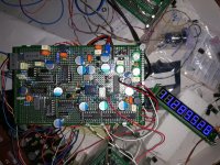
Hello, I've finally built PLL designed by Marc Heijligers and team (Guido Tent etc..) with success and with great “technical” satisfaction for me.
I say “technical” as the sonic and measured jitter improvements (see pics, a tiny -5dB jitter improvement) are subtle and the benefit-cost ratio to build this (a synchronous separate PLL clock instead of using the direct receiver MCK clock signal) is unfavourable.
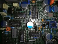
Said this, I've done also few improvements:
1) using 74AS (134 MHz) instead of 74HC (29 MHz)
2) using AD8411 as a ultra fast 4ns clock shaper
3) adopting LT1963 low noise LD voltage regulator plus BC550C low noise transistor
4) inserting a 3-24ns RC delay network in reset path (470R+ 6pF_to_50pF trimmer capacitor) plus a series of NAND gates, to make an effective way to eliminate the dead zone: the shorter the RESET delay in the PFD, the less likely that the PFD will output an incorrect decision. However, we need the RESET delay to be long enough to eliminate the DEAD-ZONE in the PFD. Thus the orange trimmer in the pic. But how to trim this?? I'm trying by randomise tempts but I feel it is unsatisfying. I've done lowering a little the harmonics on the Jitter test signal.
5) choose a higher PLL working frequency. See below
NOW THE BIG ORIGINAL QUESTION: choose the PLL working frequency (WFQ). Original scheme divides both VCXO and MCK by 16 to make the PLL working at 705.6kHZ. I've tried at :16, :8, :4 and :2. All work locking the PLL!
Few considerations of mine:
a) a lower WFQ makes the locking longer; at higher WFQ the PLL lock faster
b) I suppose that 74AS74 shorter propagation delay (vs original 74HC) allows to use higher WFQ
c) very difficult decision to choose the right WFQ, as I didn't fully understand the pro and cons
d) by ear, the :8 (1.4112MHz) and the :4 (2.8224MHz) WFQ sound slight better (but benefits are almost undetectable)
e) with a network player SPDIF input, all the mentioned WFQ work good. But with a CD player SPDIF input, the PLL get randomly unlocks for an instant after some minutes (!!!) with the usual annoying pop and clicks when using the lowest original WFQ") 16 i.e. 705.6kHZ). By using a faster WFQ 8 i.e. 1.4112MHz and up), both the machines never unlock. Hence, the decision is to skip the original design lower WFQ 16 i.e. 705.6kHZ).
16 i.e. 705.6kHZ). By using a faster WFQ 8 i.e. 1.4112MHz and up), both the machines never unlock. Hence, the decision is to skip the original design lower WFQ 16 i.e. 705.6kHZ).
f) I think that by using a lower WFQ, the PLL less - or slowly- interferes with the VCXO once locked, and this should have a benefit in term of output jitter if the VCXO is clean and well designed
Thus, I'm actually using :8 (1.4112MHz), but I would be happier if someone could kindly explain to me the pro and cons to use a faster or lower WFQ.
I say “technical” as the sonic and measured jitter improvements (see pics, a tiny -5dB jitter improvement) are subtle and the benefit-cost ratio to build this (a synchronous separate PLL clock instead of using the direct receiver MCK clock signal) is unfavourable.
Said this, I've done also few improvements:
1) using 74AS (134 MHz) instead of 74HC (29 MHz)
2) using AD8411 as a ultra fast 4ns clock shaper
3) adopting LT1963 low noise LD voltage regulator plus BC550C low noise transistor
4) inserting a 3-24ns RC delay network in reset path (470R+ 6pF_to_50pF trimmer capacitor) plus a series of NAND gates, to make an effective way to eliminate the dead zone: the shorter the RESET delay in the PFD, the less likely that the PFD will output an incorrect decision. However, we need the RESET delay to be long enough to eliminate the DEAD-ZONE in the PFD. Thus the orange trimmer in the pic. But how to trim this?? I'm trying by randomise tempts but I feel it is unsatisfying. I've done lowering a little the harmonics on the Jitter test signal.
5) choose a higher PLL working frequency. See below
NOW THE BIG ORIGINAL QUESTION: choose the PLL working frequency (WFQ). Original scheme divides both VCXO and MCK by 16 to make the PLL working at 705.6kHZ. I've tried at :16, :8, :4 and :2. All work locking the PLL!
Few considerations of mine:
a) a lower WFQ makes the locking longer; at higher WFQ the PLL lock faster
b) I suppose that 74AS74 shorter propagation delay (vs original 74HC) allows to use higher WFQ
c) very difficult decision to choose the right WFQ, as I didn't fully understand the pro and cons
d) by ear, the :8 (1.4112MHz) and the :4 (2.8224MHz) WFQ sound slight better (but benefits are almost undetectable)
e) with a network player SPDIF input, all the mentioned WFQ work good. But with a CD player SPDIF input, the PLL get randomly unlocks for an instant after some minutes (!!!) with the usual annoying pop and clicks when using the lowest original WFQ
16 i.e. 705.6kHZ). By using a faster WFQ 8 i.e. 1.4112MHz and up), both the machines never unlock. Hence, the decision is to skip the original design lower WFQ 16 i.e. 705.6kHZ).f) I think that by using a lower WFQ, the PLL less - or slowly- interferes with the VCXO once locked, and this should have a benefit in term of output jitter if the VCXO is clean and well designed
Thus, I'm actually using :8 (1.4112MHz), but I would be happier if someone could kindly explain to me the pro and cons to use a faster or lower WFQ.
Attachments

Last edited:
With a given loop filter and charge pump current, the loop bandwidth will depend on the phase comparison frequency (WFQ, in your terms). The lower the WFQ, the higher the division ratio of the feedback divider, the more the whole loop gain curve shifts down and the slower the loop response. The damping of the loop response also depends on it. It seems like the loop couldn't keep up with the drift of the output sample rate of the CD player for too low values of WFQ.
Since you apparently have a way to measure jitter, you could check what setting of the reset delay gives you least jitter. (Or have you already done that? That wasn't clear to me.) A dead zone will result in extra jitter, but an excessive reset delay will result in overlap of the up and down pulses, which results in more charge pump noise, which also causes jitter. Somewhere in between there must be an optimum. It is quite possible that the differences are too small to measure, though.
Correction: the part about charge pump noise doesn't apply since you haven't got a charge pump...
Last edited:
A dead zone will result in extra jitter, but an excessive reset delay will result iSince you apparently have a way to measure jitter, you could check what setting of the reset delay gives you least jitter. (Or have you already done that? That wasn't clear to me.)
Hi, yes I trimmed the capacitor to get the lower jitter (but slightly changed only the lower overtone harmonics) and I cannot tell you the final setting as I cannot measure the tiny capacitor set. But 10 ns (470R+22pF) should be a good start in addition to the average delay of three series 74AS00 ports (3*2.5ns=7.5ns) against the average propagation delay of the 74AS74 flip-flop (6.5ns).
Thus, it seems I found the lower limit of WFQ (like you said set by a stable locking of the drift of the output sample rate of the CD player) which is not 1:16 but 1:8.
Now how to decide which is the higher limit of WFQ? Why by ear a lower WFQ should sound better than a higher WFQ? Which is the trade-off (or best compromise)?
As long as your VCXO is better than the crystal oscillator of the signal source and as long as you don't lose lock or run into timing problems, lower loop bandwidth means better jitter suppression. You could also change loop bandwidth by redimensioning the loop filter, though.
As long as your VCXO is better than the crystal oscillator of the signal source and as long as you don't lose lock or run into timing problems, lower loop bandwidth means better jitter suppression. You could also change loop bandwidth by redimensioning the loop filter, though.
Ohh thanks , you were too much clear now!
Thanks! Hence, you confirm that having choose 1:8 is technically the best, that was in fact by ear! (as going up to 1:16 I lost sometimes the lock with some sources, so cannot use)
Now why lower loop bandwidth means better jitter suppression? That's the point now. Sorry, be so kind to clarify just this last point to me?
Jitter is essentially the same as phase noise. That is, the basic phenomenon is the same, but when you describe it in the time domain, you call it jitter, when you describe it in the frequency domain, you call it phase noise. When you connect a jittery clock signal to a very good spectrum analyser, you will see sidebands around the clock signal (close-in phase noise) and a noise floor (phase noise floor).
Looking at the transfer from the input to the output and assuming equal input and output frequencies to keep things simple, a locked PLL basically acts as a bandpass filter centred around the clock frequency. The bandwidth is roughly equal to twice the loop bandwidth (*): from one PLL loop bandwidth below to one PLL loop bandwidth above the clock frequency.
When you apply a jittery clock signal to the input of such a PLL, close-in phase noise that falls inside the passband is passed on to the output 1:1. Close-in phase noise outside the passband is attenuated, as is the noise floor. Hence, the lower the bandwidth, the more of the input phase noise is suppressed.
At the same time, the PLL acts as a high-pass filter for the phase noise of its own VCO. The smaller the loop bandwidth, the less close-in phase noise of the VCO gets suppressed and its phase noise floor isn't suppressed at all. Hence the remark in post #13 that the comment only applies when the VCXO is better than the oscillator of the signal source.
(*): With loop bandwidth I mean the frequency at which the magnitude of the loop gain becomes 1, not to be confused with the open loop bandwidth, which is 0 in a PLL.
Last edited:
Thank you MarcelvgG, very exhaustive explanation, my compliments!
Then scenario is now much clearer.
Hence, let me try to summarize:
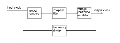
Let us assume that "1: N" dividers drops the control bandwidth of the PLL by "N", making the PLL "N" times slower.
First at all, we need to define which should be the main goal of the PLL in our DAC.
Since the digital signals generated by a S/PDIF receiver, like CS8412, have a high intrinsic jitter level (mainly because the inner PPL is not crystal-based), our purpose is to recover the output serial data by re-cloking the signals just before entering the DAC chip.
To do this we can use D flip-flops to realign the edges of the digital outputs of the receiver to the edges of a new, much more stable, local clock. We call this: "local VCXO clock".
Also, we need to define what is "Jitter": jitter is the unwanted fluctuation (variance) of a defined clock point and we can divide it into two major groups. The first is the "short-term period jitter": it is measured by the high frequency movement of the point from its ideal position in adjacent clock cycles. The second type of jitter is the "long term jitter" which is measured over a much longer period (in cycles or seconds). We call this also "frequency drift".
In general, PLL output jitter is dominated by three noise sources: the transferred jitter of the receiver, the generated noise of the local VCXO clock and the added phase noise of the components engaged in the PLL.
The local VCXO clock, in order to realign with precision each and every rising/falling edges of the receiver's serial output, must be: 1) "short-term jitter-free", i.e. stable in high-frequency and 2) "long-term synchronized" to the receiver, in order to prevent random "clicks and pops" due to the fact that the recovered signals at different timings do not meet any longer setup and hold time requirements of the DAC. For this purpose, the VCXO clock has to follow the frequency drift of the receiver: be aware that these "long term jitter adjustments" are inaudible only if done slowly, below the human hearing range.
Thus, the goal of our PLL is not to treat the "short term jitter" of the VCXO clock. The local VCXO clock must be intrinsically high frequency jitter-free by using a good design and construction. In our circuit I have used a chain of low-noise low-dropout voltage regulators in power supply, a stable JFet Colpitts crystal-based oscillator, an ultra-fast comparator to sharp the signal, an engineered layout of the components on the board.
On the contrary, the main goal of the PLL is to phase the "long term jitter" of the VCXO to the frequency drifts of the receiver (and, therefore, of the transport). In simple words our PLL has only to synchronize the VCXO clock to the receiver, by pulling and pushing it slowly in order to make run it at identical frequency and phase of the receiver. We do not care about the "high frequency" jitter components of the clocks: it is our local VCXO clock that will drive the re-clock and this is supposed to be already high frequency jitter free!
In conclusion, the PLL must ignore short term differences (or “fast” errors), whilst tracking slower long-term frequency fluctuations (or “slow” errors).
A "slow" (narrowband) PLL is the best choice because all but the lowest-frequency jitter of the receiver is rejected: in fact, if the reference clock has a significant amount of jitter, the typical remedy is to use a narrow PLL bandwidth to filter out this noise. Operating in this way, the PLL will not propagate any "short term period jitter" present in the input, but neither will be able to correct any “fast” error committed by the VCXO clock. Hence, the last need to be clean and stable in high frequency.
On the other hand, "fast" (wideband) PLL causes the loop to respond quickly to the high frequency noise being injected by the VCXO and compensate for it: simply, it is able to adjust for this noise and counteract it. But a "fast" PLL is also harder to control. It might over-adjust, increasing output noise and jitter. If the loop bandwidth is too high then incoming high frequency jitter can be passed to the output or even being slightly amplified due to jitter peaking: a "fast" PLL must only be used when the clock of the receiver is clean and stable in high frequency, which is not our case.
So:
1) the slower the PLL, the higher the division ratio of the two dividers, the higher the cost and the complexity of the circuit. This is a "Cons".
2) the slower the PLL, the less rapid the circuit switches, the lower the radiated electrical noise generated into the nearby circuitry due to capacitive coupling, radiated coupling, and inductive coupling. This is a "Pro".
3) the slower the PLL, the higher the allowed propagation delay of the components engaged in the PLL (in particular the flip-flops). This is a "Pro".
4) the slower the PLL, the higher the division ratio of the two dividers, the higher is the additive noise source at their output into the loop path. This is a "Cons".
5) the slower the PLL, the slower the PLL can adjust the output frequency, the slower is the lock time: this is why using 1:16 my PLL take much more time to lock. This is a "Cons".
6) the slower the PLL, the slower the PLL response, the higher the probability that PLL run into timing problems as it cannot "follow" the reference drift: this is why using 1:16 my PLL sometime loses the lock with old players. This is a "Cons".
7) the slower the PLL, the more high-frequency phase noise of the input reference clock is filtered out. This is of course a "Pro".
8) the slower the PLL, the higher the contribution of VCXO noise to the PLL's output jitter, because high-frequency VCXO phase noise is passed to the output since the tracking speed is too low. This is a "Cons" unless the PLL mounts a very low phase noise local VCXO.
Hence, a part of complexity, cost, additional components noise, locking time, locking stability and RF coupled noise, the main compromise between a slower or faster PLL is given by the balance in the sum of the transferred jitter from the "dirty" input clock source and the jitter generated by the "clean" internal VCXO clock.
As a rule of thumb, the balance suggests having the SLOWER PLL POSSIBLE, but compatible to a stable locking during listening and to an effective jitter-free construction of the VCXO clock.
Therefore, my decision to stay with a 1:8 divisor PLL loop in the DAC (PLL working at 1.4112MHz), which is also the best sounding to me “by ear”.
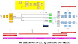
Here below the draft of the working prototype which I've already built, tested and heavenly sounding now.
One year of project thanks to many diyAudio contributors like you!
Just to finalize power supplies and stuff everything into a nice cabinet.
Any additional input and confirm are very welcome.
Thanks
Gianluca G.
___________
Then scenario is now much clearer.
Hence, let me try to summarize:
Let us assume that "1: N" dividers drops the control bandwidth of the PLL by "N", making the PLL "N" times slower.
First at all, we need to define which should be the main goal of the PLL in our DAC.
Since the digital signals generated by a S/PDIF receiver, like CS8412, have a high intrinsic jitter level (mainly because the inner PPL is not crystal-based), our purpose is to recover the output serial data by re-cloking the signals just before entering the DAC chip.
To do this we can use D flip-flops to realign the edges of the digital outputs of the receiver to the edges of a new, much more stable, local clock. We call this: "local VCXO clock".
Also, we need to define what is "Jitter": jitter is the unwanted fluctuation (variance) of a defined clock point and we can divide it into two major groups. The first is the "short-term period jitter": it is measured by the high frequency movement of the point from its ideal position in adjacent clock cycles. The second type of jitter is the "long term jitter" which is measured over a much longer period (in cycles or seconds). We call this also "frequency drift".
In general, PLL output jitter is dominated by three noise sources: the transferred jitter of the receiver, the generated noise of the local VCXO clock and the added phase noise of the components engaged in the PLL.
The local VCXO clock, in order to realign with precision each and every rising/falling edges of the receiver's serial output, must be: 1) "short-term jitter-free", i.e. stable in high-frequency and 2) "long-term synchronized" to the receiver, in order to prevent random "clicks and pops" due to the fact that the recovered signals at different timings do not meet any longer setup and hold time requirements of the DAC. For this purpose, the VCXO clock has to follow the frequency drift of the receiver: be aware that these "long term jitter adjustments" are inaudible only if done slowly, below the human hearing range.
Thus, the goal of our PLL is not to treat the "short term jitter" of the VCXO clock. The local VCXO clock must be intrinsically high frequency jitter-free by using a good design and construction. In our circuit I have used a chain of low-noise low-dropout voltage regulators in power supply, a stable JFet Colpitts crystal-based oscillator, an ultra-fast comparator to sharp the signal, an engineered layout of the components on the board.
On the contrary, the main goal of the PLL is to phase the "long term jitter" of the VCXO to the frequency drifts of the receiver (and, therefore, of the transport). In simple words our PLL has only to synchronize the VCXO clock to the receiver, by pulling and pushing it slowly in order to make run it at identical frequency and phase of the receiver. We do not care about the "high frequency" jitter components of the clocks: it is our local VCXO clock that will drive the re-clock and this is supposed to be already high frequency jitter free!
In conclusion, the PLL must ignore short term differences (or “fast” errors), whilst tracking slower long-term frequency fluctuations (or “slow” errors).
A "slow" (narrowband) PLL is the best choice because all but the lowest-frequency jitter of the receiver is rejected: in fact, if the reference clock has a significant amount of jitter, the typical remedy is to use a narrow PLL bandwidth to filter out this noise. Operating in this way, the PLL will not propagate any "short term period jitter" present in the input, but neither will be able to correct any “fast” error committed by the VCXO clock. Hence, the last need to be clean and stable in high frequency.
On the other hand, "fast" (wideband) PLL causes the loop to respond quickly to the high frequency noise being injected by the VCXO and compensate for it: simply, it is able to adjust for this noise and counteract it. But a "fast" PLL is also harder to control. It might over-adjust, increasing output noise and jitter. If the loop bandwidth is too high then incoming high frequency jitter can be passed to the output or even being slightly amplified due to jitter peaking: a "fast" PLL must only be used when the clock of the receiver is clean and stable in high frequency, which is not our case.
So:
1) the slower the PLL, the higher the division ratio of the two dividers, the higher the cost and the complexity of the circuit. This is a "Cons".
2) the slower the PLL, the less rapid the circuit switches, the lower the radiated electrical noise generated into the nearby circuitry due to capacitive coupling, radiated coupling, and inductive coupling. This is a "Pro".
3) the slower the PLL, the higher the allowed propagation delay of the components engaged in the PLL (in particular the flip-flops). This is a "Pro".
4) the slower the PLL, the higher the division ratio of the two dividers, the higher is the additive noise source at their output into the loop path. This is a "Cons".
5) the slower the PLL, the slower the PLL can adjust the output frequency, the slower is the lock time: this is why using 1:16 my PLL take much more time to lock. This is a "Cons".
6) the slower the PLL, the slower the PLL response, the higher the probability that PLL run into timing problems as it cannot "follow" the reference drift: this is why using 1:16 my PLL sometime loses the lock with old players. This is a "Cons".
7) the slower the PLL, the more high-frequency phase noise of the input reference clock is filtered out. This is of course a "Pro".
8) the slower the PLL, the higher the contribution of VCXO noise to the PLL's output jitter, because high-frequency VCXO phase noise is passed to the output since the tracking speed is too low. This is a "Cons" unless the PLL mounts a very low phase noise local VCXO.
Hence, a part of complexity, cost, additional components noise, locking time, locking stability and RF coupled noise, the main compromise between a slower or faster PLL is given by the balance in the sum of the transferred jitter from the "dirty" input clock source and the jitter generated by the "clean" internal VCXO clock.
As a rule of thumb, the balance suggests having the SLOWER PLL POSSIBLE, but compatible to a stable locking during listening and to an effective jitter-free construction of the VCXO clock.
Therefore, my decision to stay with a 1:8 divisor PLL loop in the DAC (PLL working at 1.4112MHz), which is also the best sounding to me “by ear”.
Here below the draft of the working prototype which I've already built, tested and heavenly sounding now.
One year of project thanks to many diyAudio contributors like you!
Just to finalize power supplies and stuff everything into a nice cabinet.
Any additional input and confirm are very welcome.
Thanks
Gianluca G.
___________
Attachments
Last edited:
metastability
Yesterday I did two changes. One successful and the other worse.
I realized that since I'm using synchronous counter as a divisor in the path (74AS169), which is fed by the VCXO (11.2896 MHz), I have for free available pins in the counter sourcing submultiples jitter-free synchronous frequencies, in particular 5.6MHz and 2.8MHz clock signals.
The serial data I'm going to recover (re-clock) are SCK which runs at 2.8MHz, FSYNC which runs at 44.1MHz and SDATA which should run at submultiples of SCK, depending on music streaming.
So, being the highest frequency to re-clock 2.8MHz, why not recover the serial data with a lower frequency, i.e. 5.6MHz or even 2.8MHz ??
Then I tried to clock the three flip-flops in the re-clock circuit with 5.6MHz and 2.8MHz clock signals, instead of 11.2896MHz.
2.8MHz, didn’t produce any sound at all, as per theory: and in fact the minimum clock rate in a D flip-flop should be at least the double of the rate of the input data (SCK at 2.8MHz). If we use a clock with the same rate of the signal to recover, the output will be mute (either high level or low level, depending on the phase of the clock in input of the 7474 flip flop).
5.6MHz signal re-clock worked perfect without any “clicks and pops”, as per theory being double of the highest rate of the input data (SCK at 2.8MHz). But jitter was slightly worse (nearly negligible difference, but in any case worse), probably due to the additional jitter of the 74AS169 counter in the re-clock signal path; thus, I decided to maintain the original 11.2896MHz re-clock signal.
The second change I tried was to invert the re-clock signal (always at 11.2896 MHz), by simply using the inverting unused pin of the AD8611 comparator in the VCXO, that should run now at the same frequency but 180° un-phased in respect to the input MCK signal once the PLL will lock VCXO in phase to MCK.
Well, in effect this worked particularly better and jitter looks disappeared nearly at all (also with the help of the PLL trimming of the delay circuit). This probably worked the best as should avoid any possible flip-flop metastability which may produce jitter at its output due to the misunderstood level of the data triggered by a “synchronous” positive egde of the clock: now all the positive edges of the re-clock signal should be always un-phased to any positive edge of the three signals in input to be recovered.
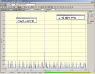
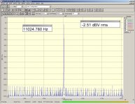
Attached the final jitter measured result.
Gianluca G.
Yesterday I did two changes. One successful and the other worse.
I realized that since I'm using synchronous counter as a divisor in the path (74AS169), which is fed by the VCXO (11.2896 MHz), I have for free available pins in the counter sourcing submultiples jitter-free synchronous frequencies, in particular 5.6MHz and 2.8MHz clock signals.
The serial data I'm going to recover (re-clock) are SCK which runs at 2.8MHz, FSYNC which runs at 44.1MHz and SDATA which should run at submultiples of SCK, depending on music streaming.
So, being the highest frequency to re-clock 2.8MHz, why not recover the serial data with a lower frequency, i.e. 5.6MHz or even 2.8MHz ??
Then I tried to clock the three flip-flops in the re-clock circuit with 5.6MHz and 2.8MHz clock signals, instead of 11.2896MHz.
2.8MHz, didn’t produce any sound at all, as per theory: and in fact the minimum clock rate in a D flip-flop should be at least the double of the rate of the input data (SCK at 2.8MHz). If we use a clock with the same rate of the signal to recover, the output will be mute (either high level or low level, depending on the phase of the clock in input of the 7474 flip flop).
5.6MHz signal re-clock worked perfect without any “clicks and pops”, as per theory being double of the highest rate of the input data (SCK at 2.8MHz). But jitter was slightly worse (nearly negligible difference, but in any case worse), probably due to the additional jitter of the 74AS169 counter in the re-clock signal path; thus, I decided to maintain the original 11.2896MHz re-clock signal.
The second change I tried was to invert the re-clock signal (always at 11.2896 MHz), by simply using the inverting unused pin of the AD8611 comparator in the VCXO, that should run now at the same frequency but 180° un-phased in respect to the input MCK signal once the PLL will lock VCXO in phase to MCK.
Well, in effect this worked particularly better and jitter looks disappeared nearly at all (also with the help of the PLL trimming of the delay circuit). This probably worked the best as should avoid any possible flip-flop metastability which may produce jitter at its output due to the misunderstood level of the data triggered by a “synchronous” positive egde of the clock: now all the positive edges of the re-clock signal should be always un-phased to any positive edge of the three signals in input to be recovered.
Attached the final jitter measured result.
Gianluca G.
Attachments
Last edited:
- Status
- This old topic is closed. If you want to reopen this topic, contact a moderator using the "Report Post" button.
- Home
- Source & Line
- Digital Line Level
- Understanding PLL: why PLL design need a frequency divider?