Hello,
Could you please check the following reclock schemes which I’ve implemented with more or less success and kindly give me some advice.
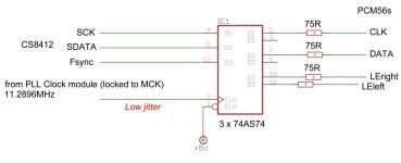
Number 1 (reclock all the 3 lines), should be the most logical way, and in effect it does work with a PLL but very difficult as it give me too much POPs and RF noise before locking MCK. Also Jitter looks not good as 2) and 3)
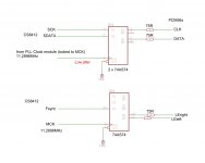
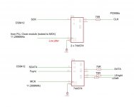
Number 2 works good with a PLL and it is much easier to implement (less POPS and RF noise before locking MCK). Number 3 is even easier (nearly no POPS and RF noise at all even in a larger PLL lock frequency zone), but in this way I’m going to re-clock only SCK signal.
Do you think that to reclock as picture 2 (i.e. only SCK and SDATA, and leave FSYNC be reclocked by dirty CS8412 MCK) can be the correct (and best) way?
Or just relocking only SCK with a low jitter PLL (locked to MCK) is worth and enough (as picture 3)?
(FYI CS8412 can work only is a master mode when piloting PCM56, because there is no slave mode for Mode 5 Out, L/R, 16 Bits LSBJ, required by PCM56 protocol)
Thanks!
attachements...
Could you please check the following reclock schemes which I’ve implemented with more or less success and kindly give me some advice.
Number 1 (reclock all the 3 lines), should be the most logical way, and in effect it does work with a PLL but very difficult as it give me too much POPs and RF noise before locking MCK. Also Jitter looks not good as 2) and 3)
Number 2 works good with a PLL and it is much easier to implement (less POPS and RF noise before locking MCK). Number 3 is even easier (nearly no POPS and RF noise at all even in a larger PLL lock frequency zone), but in this way I’m going to re-clock only SCK signal.
Do you think that to reclock as picture 2 (i.e. only SCK and SDATA, and leave FSYNC be reclocked by dirty CS8412 MCK) can be the correct (and best) way?
Or just relocking only SCK with a low jitter PLL (locked to MCK) is worth and enough (as picture 3)?
(FYI CS8412 can work only is a master mode when piloting PCM56, because there is no slave mode for Mode 5 Out, L/R, 16 Bits LSBJ, required by PCM56 protocol)
Thanks!
attachements...
Attachments
It's not apparent to me why your three proposed implementations should differ in the degree of 'popping' noise you hear, assuming, proper supply noise decoupling of each 74AS74 chip. That said, the only reason I can readily think for why your circuit produces 'pops' at all is that the MCK signal fed the 74AS74 chips is not correctly phased with respect to the signals being re-clocked. Some PLL circuit implementations will frequency-lock but not phase-lock. A quick test of your clock-module to find whether it is the culprit would be to bypass it and feed the CS8412's MCLK signal directly to the 7AS74 chips. Listen for whether that eliminates the pops.
Back to your three 74AS74 implementation choices. Assuming that the data conversion instant for the PCM56 is triggered synchronous with the FSYNC signal (which, I believe it is), best should be re-clocking FSYNC via it's own dedicated 74AS74 chip. That should incur the least chip supply noise induced jitter of the three implementations. Worst, would be re-clocking both FSYNC and DATA via the same 74AS74 chip. Which has the potential to induce data correlated jitter.
Not that you should actually hear, nor even achieve, any difference among the three approaches. Jitter reduction question are diffcult to accurately answer without instrumented measurement.
Last edited:
It's not apparent to me why your three proposed implementations should differ in the degree of 'popping' noise you hear, assuming, proper supply noise decoupling of each 74AS74 chip. That said, the only reason I can readily think for why your circuit produces 'pops' at all is that the MCK signal fed the 74AS74 chips is not correctly phased with respect to the signals being re-clocked. Some PLL circuit implementations will frequency-lock but not phase-lock. A quick test of your clock-module to find whether it is the culprit would be to bypass it and feed the CS8412's MCLK signal directly to the 7AS74 chips. Listen for whether that eliminates the pops.
Back to your three 74AS74 implementation choices. Assuming that the data conversion instant for the PCM56 is triggered synchronous with the FSYNC signal (which, I believe it is), best should be re-clocking FSYNC via it's own dedicated 74AS74 chip. That should incur the least chip supply noise induced jitter of the three implementations. Worst, would be re-clocking both FSYNC and DATA via the same 74AS74 chip. Which has the potential to induce data correlated jitter.
Not that you should actually hear any difference among the three approaches. Jitter reduction question are nearly impossible to accurately answer without instrumented measurement.
Thanks for the reply. PLL is not built yet: i'm just manually trimmering the varicap in serie with crystal of my clock and POP dissapper as soon as I reach MCK frequency. I will use this PLL scheme: Google Image Result for http://www.audiocostruzioni.com/a_d/elettroniche/elettroniche-varie/dac-II-maurizio-daniele/PLL.jpg as soon as I will decide what to reclock. No idea if this is also phase-lock or just frequency-lock. As it will change the voltage of the varicap (like I'm doing manually now) in serie to my crystal I think that it is frequency-lock only. In fact how I could change phase too if i just change the crystal frequency with a varicap??
Thus this could be a problem if only frequency-lock in effect..
The 3 lines are reclocked by one 74as74 each, and they work perfectly if I just feed simultanely the 3 latch with MCK. This is the reason why I'm wondering why reclocking just SCK and SDATA gives to me better result and stability.
I can really measure Jitter with J-test signal and the best result I got is reclocking only SDATA and SCK.
So question is: is really necessary to reclock Fsync too? I suppose that SCK is the most important line to be free of jitter. And after that, SDATA must be clean too. Fsync select only the channel, so why reclock also this?
As far as I know, the most important is the LE (latch enable) signal. Bit clock or SCK is just for shift register inside DAC. The most critical point is the where the conversion starts and that's triggered by LE signal. I'd recommend using another flip-flop for the LE signal.
Poting
Poting
trying to lower CS8412 jitter?
If you try to upgrade your overall dac quality - I would point out to try to Implement a modern digital receiver with better quality - like AK4113 / 4118 - that way you can go with 192 KHz Input - also you can have a choice for other sources than one spdif and display
Also you can check out @ .3lite new 16 x digital Interpolation filter which can take directly I2S from AK4113
Hello,
Could you please check the following reclock schemes which I’ve implemented with more or less success and kindly give me some advice.
Number 1 (reclock all the 3 lines), should be the most logical way, and in effect it does work with a PLL but very difficult as it give me too much POPs and RF noise before locking MCK. Also Jitter looks not good as 2) and 3)
Number 2 works good with a PLL and it is much easier to implement (less POPS and RF noise before locking MCK). Number 3 is even easier (nearly no POPS and RF noise at all even in a larger PLL lock frequency zone), but in this way I’m going to re-clock only SCK signal.
Do you think that to reclock as picture 2 (i.e. only SCK and SDATA, and leave FSYNC be reclocked by dirty CS8412 MCK) can be the correct (and best) way?
Or just relocking only SCK with a low jitter PLL (locked to MCK) is worth and enough (as picture 3)?
(FYI CS8412 can work only is a master mode when piloting PCM56, because there is no slave mode for Mode 5 Out, L/R, 16 Bits LSBJ, required by PCM56 protocol)
Thanks!
attachements...
As far as I know, the most important is the LE (latch enable) signal. ... The most critical point is the where the conversion starts and that's triggered by LE signal.
Poting
Oh, man,... re-reading the DAC datatsheet I think you are 100% right. I'm going to re-clock fsync first and see..
...I can really measure Jitter with J-test signal and the best result I got is reclocking only SDATA and SCK...
That result suggests to me that your re-clocking circuit is likely making jitter worse. Which is why not re-clocking the FSYNC signal meaures better than re-clocking it. Your re-clocking circuit is probably making DATA and SCK signal jitter worse as well, but neither happens to be critical for jitter. I believe that FSYNC is the key clock signal regarding jitter, as far as the PCM56 is concerned.
Last edited:
As far as I know, the most important is the LE (latch enable) signal. ... The most critical point is the where the conversion starts and that's triggered by LE signal.
Poting
Oh, man,... re-reading the DAC datatsheet I think you are 100% right. I'm going to re-clock fsync first and see..
- Status
- This old topic is closed. If you want to reopen this topic, contact a moderator using the "Report Post" button.
- Home
- Source & Line
- Digital Line Level
- DAC receiver reclock: help to close my project