I would have star grounded them too.I would have thought it best to keep them separate up to the 0v pcb connection to the psu, or even connect the two grounds direct to the psu separately.
I don't care who wrote it, there is so much conflicting information out there.
Surely it depends on what it is you are trying to accomplish, the absolute lowest EMI, or isolation?
It could very well be that the lowest impedance return path would be right where the supposed inductor is suggested to go. But if the currents are allowed to flow there the digital noise disturbs the linearity of the analogue stages.
The point of the inductor isn't to minimise EMI it's to deliberately stop current from flowing where it's going to reduce performance elsewhere. I'm guessing that this is seen as a trade off. Increase EMI in a low power circuit but improve absolute performance elsewhere.
Whether or not this design process is strictly necessary is another thing entirely.
On my DAC boards I would aim to keep the digital ground from polluting the analogue ground which may lead to worse SQ. (I'm less concerned about RF interference emission)
Its probably a moot point with such a simple design, no digital tracks running around the board, signals are 3.3v not the 5v expected. and the max frequency is 2.8Mhz.
So I'm leaning towards substantial top & bottom parallel digital ground traces and top & bottom ground planes for the analogue with separate connections to the psu star ground + many vias from top to bottom planes, especially under the dacs.
If two-layer and multiple DAC chips, I would use seperate planes that don't overlap (so, one side of the PCB only) and with sufficient clearance to avoid inductive coupling, then connect the planes with stubs right under the chips to have the "quick" return paths for the internal currents between the IC's analog and digital sections. Supply bypass caps mounted close to the chip and returning to their correct plane.
For the actual layout process I personally always draw explicit GND returns first for each trace right under/beneath it, no matter if signal or supply, later fill up the planes.
And always place damping resistors (33R or so) in each and every digital I/O line to control the signal edge rate.
For the actual layout process I personally always draw explicit GND returns first for each trace right under/beneath it, no matter if signal or supply, later fill up the planes.
And always place damping resistors (33R or so) in each and every digital I/O line to control the signal edge rate.
Last edited:
If two-layer and multiple DAC chips, I would use seperate planes that don't overlap (so, one side of the PCB only) and with sufficient clearance to avoid inductive coupling, then connect the planes with stubs right under the chips to have the "quick" return paths for the internal currents between the IC's analog and digital sections. Supply bypass caps mounted close to the chip and returning to their correct plane.
For the actual layout process I personally always draw explicit GND returns first for each trace right under/beneath it, no matter if signal or supply, later fill up the planes.
And always place damping resistors (33R or so) in each and every digital I/O line to control the signal edge rate.
The trouble is, most pcb manufacturers do not want to etch off large areas of copper so I am probably stuck with overlapping planes. I'll look into segmenting the planes so overlaps are always of the same ground ie Agnd or Dgnd so they do not overlap each other.
That means two wires for digital and analog grounds; but joined together at power supply site? Or joined together at the DAC site?
Join them at the dacs, is what I would suggest.
Join them at the dacs, is what I would suggest.
Or join at psu end and together at the dac though a ferrite bead?
@Markw4
@batteryman
It depends on if you have separate bridges/transformer or not.
You may have separate Vregs (for ANA and DIG) but same bridge (and trafo): in this case you have one common ground at PSU. In this case if we tie two wires (for ANA and DIG) after the respective Vreg CAPs, and we join them at DAC level with ferrite bead or direct solder, we would form a ground loop.
Hence, or we tie a unique ground wire and we join it at ANA and DIG DAC pins or we tie two wires but without joining them at the DAC pins.
Otherwise we shoud have separate bridges (and even transformers) for ANA and DIG and in this case makes sense to tie two wires till DAC and join together without ferrite bead: i think this solution is the best using wires even if the most expensive: no groud loops at all.
Is this correct?
Last edited:
Why join them at the PSU end? Suppose you ran them on sets of batteries, why would it matter it you connected the batteries together wherever they are? On the other hand, the dac chips want them at exactly the same voltage at the dac chip pins.
Yes, that's a point. I plan to use 6 sets of batteries at some stage (3 per dac chip)
@Markw4
@batteryman
It depends on if you have separate bridges/transformer or not.
Sure. Then your problem statement should include that you have some existing coupling at the power supply end. Then you could decide if you need to do some engineering work at that end to get your system performance where you want it.
Surely it depends on what it is you are trying to accomplish, the absolute lowest EMI, or isolation?
It could very well be that the lowest impedance return path would be right where the supposed inductor is suggested to go. But if the currents are allowed to flow there the digital noise disturbs the linearity of the analogue stages.
The point of the inductor isn't to minimise EMI it's to deliberately stop current from flowing where it's going to reduce performance elsewhere. I'm guessing that this is seen as a trade off. Increase EMI in a low power circuit but improve absolute performance elsewhere.
Whether or not this design process is strictly necessary is another thing entirely.
You need to ask yourself why high frequency currents are deemed to be a problem, when they return in the most predictable manner. Only the I2S and I2C/SPI interface currents are flowing there anyway. There is no problem to solve unless you have done stupid stuff like put a DSP in the middle of the analog side of the board. In fact, low frequency return currents are going to spread on the reference plane to a much greater degree.

Of course, there will be lower frequency content in the return as well, but an inductor isn't going to help with that... maybe cap stitching the planes would work if you were trying to isolate from low frequency noise but still maintain an RF connection.
Connecting the planes with an inductor is a BAD idea.
Grounding Converters | Analog Devices
"But they must be joined at the package(1) and nowhere else.
(1): And with the lowest possible impedance – do not separate them with resistors, inductors or ferrite beads. "
"sometimes a converter data sheet may recommend that AGND and DGND are connected to system analog and digital grounds respectively. When a data sheet tells you to do this it is incorrect, and you should ignore it."
Grounding of Mixes Signal Systems
Last edited:
No. There is no need for separate supplies or supply GND returns. You simple make the impedance of supply feeds to the local (on-board) regulators high impedance (series resistors will do in almost all cases) so that GND connections under the DACs dominate the scene. And were do we put the supply connector on the board, etc? Avoiding to elaborate here I just recommend everybody get a copy of H.W.Ott's "Electromagnetic Compatibility Engineering", this is the best available textbook on EMC and Signal Integrity and answer absolutely all questions about grounding in this thread as well as the gazillion of similar threads. It actually covers every single detail you need to know from basic electrical circuits theory (most design errors start right there) to the layout of a proper PCB to the design of a complete flaw-less product with supplies, enclosure, internal cabling etc.Is this correct?
Sometimes it makes sense to use separate supplies because analog needs +-15v and digital needs 5v or 3.3v. Doesn't usually make a lot of sense to drop +15 to +3.3 with onboard reguators, for various reasons. However, those separate power supplies exist in the first place for reasons other than grounding. Since they do exist, their separation can be used as is convenient.
built!
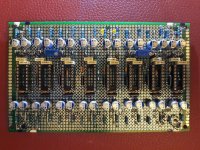
Hello, just built the PCM56 board but not tested yet.... Four PCM56 in parallel, left and right channel.
I've decided to create two separate power supply boards with separate transformers, bridges and regulators, one for analog circuitry (+/-5V) and one for digital (+/-5V).
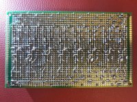
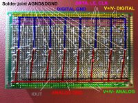
A/D Grounds are joint at each chip level as manufactures are suggesting: I unfortunately formed in this way multiple small ground loops due to the parallel DAC configuration, but this can be also seen as a Ground network plane, hope with some benefits.
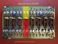
Analog and digital signals are fully separated in the board. Each chip's power supply is filtered with a RCLC network (R damping= 1 ohm, C=22uF OS-CON, L= ferrite bead, C=100nF or 220nF ceramic for digital, polyester for analog).
That was the best I could design for 8 chips in 10x15 cm perfboard. I would not expect any digital noise at all. I'm just a little worry if the 1 ohm damping series resistors will badly influence the sound or dynamic (but without the simulation has shown a huge resonance peak in the 1MHz area!)
Sockets are mandatory as I need to select the eight DAC chips one by one for the lowest THD (PCM56-S)
Pics are four but board is just one.
Hello, just built the PCM56 board but not tested yet.... Four PCM56 in parallel, left and right channel.
I've decided to create two separate power supply boards with separate transformers, bridges and regulators, one for analog circuitry (+/-5V) and one for digital (+/-5V).
A/D Grounds are joint at each chip level as manufactures are suggesting: I unfortunately formed in this way multiple small ground loops due to the parallel DAC configuration, but this can be also seen as a Ground network plane, hope with some benefits.
Analog and digital signals are fully separated in the board. Each chip's power supply is filtered with a RCLC network (R damping= 1 ohm, C=22uF OS-CON, L= ferrite bead, C=100nF or 220nF ceramic for digital, polyester for analog).
That was the best I could design for 8 chips in 10x15 cm perfboard. I would not expect any digital noise at all. I'm just a little worry if the 1 ohm damping series resistors will badly influence the sound or dynamic (but without the simulation has shown a huge resonance peak in the 1MHz area!)
Sockets are mandatory as I need to select the eight DAC chips one by one for the lowest THD (PCM56-S)
Pics are four but board is just one.
Attachments

Analog and digital signals are fully separated in the board. Each chip's power supply is filtered with a RCLC network (R damping= 1 ohm, C=22uF OS-CON, L= ferrite bead, C=100nF or 220nF ceramic for digital, polyester for analog).
That was the best I could design for 8 chips in 10x15 cm perfboard. I would not expect any digital noise at all. I'm just a little worry if the 1 ohm damping series resistors will badly influence the sound or dynamic (but without the simulation has shown a huge resonance peak in the 1MHz area!)
Instead of a resistor in series with the inductor, you could try an RC series network (or a cheap aluminium electrolytic with substantial ESR) in parallel with the capacitor. The frequency-dependent losses of the ferrite bead may also help to some extent, although most ferrite beads are still mainly inductive around 1 MHz.
Edit: I didn't realize yet that your caps are already electrolytics... Did you model their losses in your simulation?
Last edited:
Instead of a resistor in series with the inductor, you could try an RC series network (or a cheap aluminium electrolytic with substantial ESR) in parallel with the capacitor. The frequency-dependent losses of the ferrite bead may also help to some extent, although most ferrite beads are still mainly inductive around 1 MHz.
Edit: I didn't realize yet that your caps are already electrolytics... Did you model their losses in your simulation?
Hi, the resonance in the MHz area to smooth with the 1 ohm resistor is formed by the ferrite plus 100/220nF capacitor, not by the big 22uF electrolytic cap.
I think the nut in the shell is to not allow digital current carrying GND conductors, be it power supply return current or digital signal return current, to become any part of the analog circuit. To achieve this goal we need to examine the physical current loops and make GND plane slits or separations accordingly. It is also important to place ceramic SMD bypass capacitors closets across the power pins and the associated GND pins of the chip, so that the capacitor shunts a current loop to its minimum physical size with respect to the higher frequency components in the current.
- Status
- This old topic is closed. If you want to reopen this topic, contact a moderator using the "Report Post" button.
- Home
- Source & Line
- Digital Line Level
- Do you really tie Analog GND and Digital GND at pin chip level in DAC/Receivers