My pcb design software generates upper and lower ground planes automatically but dividing these into separate areas is more work so I have, in the past, kept the ground planes, analogue, digital and power supply grounds all separate up to the common point at the off board 0v pin. (ie the ground planes weren't connected to anything except each other)
Multi-layer boards are great. I just wish they weren't so costly as compared to double-sided boards. So, for DIY, I usually end up having to squeeze every design in to a double-sided form.
Last edited:
Sorry, I forget to say that i'm using exclusively perfboards and not PCB...
Hence, not possible for me to create ground planes but I can only tie multiple wires and create multiple transformer/bridge ground separated power supplies

We create ground planes with perfboard all the time. Use copper foil for that. An example can be found in the instructions for building an ES9038Q2M output stage board here: Dropbox - Output Stage Instructions.zip
I would use separate ones but connect a low value inductor between them at the pcb. This keeps HF noise from getting from one to the other, whilst maintaining them at the same DC potential.
I wouldn't. Unless you want it to radiate.
Why do people think stopping the current from returning where it wants to go is a good idea?
Sorry, I forget to say that i'm using exclusively perfboards and not PCB...
Hence, not possible for me to create ground planes but I can only tie multiple wires and create multiple transformer/bridge ground separated power supplies
How about dead bug style build-up on a single-sided copper-clad board (that is, unetched PCB) or simply on a beer or soft drink can that's been cut open? That's not ideal for a DAC, but at least it gives you a solid ground plane.
How about dead bug style build-up on a single-sided copper-clad board (that is, unetched PCB)
An effective variation on that theme is to use a single sided copper clad board and then glue on it smaller pieces of the same for power lines and so on. Search for "Manhattan style" prototyping.
I know the technique, but had never heard of the term Manhattan style. Another variant uses pieces of board with copper traces on 2.54 mm pitch to solder DIL ICs and other components on, after those pieces are glued to a copper-clad board. That requires etching of those pieces of board, though.
Maybe you could even use pieces of perfboard for it and either make sure that the component leads do not stick through the holes, or rely on the glue layer as insulator (if the voltage is not too high).
Maybe you could even use pieces of perfboard for it and either make sure that the component leads do not stick through the holes, or rely on the glue layer as insulator (if the voltage is not too high).
Attachments
Last edited:
Sorry, I forget to say that i'm using exclusively perfboards and not PCB...
Hence, not possible for me to create ground planes but I can only tie multiple wires and create multiple transformer/bridge ground separated power supplies
So question is:
should I have two ground wires (digital and analog) from Power supply (transformer/bridge ground separated?) to the dac/receiver digital and analog ground pins
or
one wire from power supply to the dac/receiver joined digital and analog pins?
Method of Applying a Copper Ground Plane to Strip-board (e.g. Veroboard): 10 Steps
//
Thanks for all kind replies and for the "Manhattan"/copper tips!
But, I'm going to build a dac with 4 PCM56 in parallel, thus eight 16-pin chips, each of them with +/-5V analog and +/-5V digital.
So I have: 4 wires for power supply, 1 or 2 wires for grounds (depend on this thread), 4 wires for inputs, one wire for current output, plus some trimming resistors.
Multiply this by eight (4 x 2 channels) and put on a 15X10 cm board, plus decoupling capacitors, ferrites, input/output pin. And this is excluding receiver, separate power supplies, PLL re-clock and analogue stage which are all on different boards with separate transformer (my DAC is becoming a “cupboard”, but I’m happy the same for the result I’m getting…)
The only way to use a copper plane would be stacking the PCM56 chips, which works (I tested!), but I don't like soldering chips one over the other in a definitive project. I need also to roll and select them for the lowest MSB THD.
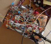
I have to stay on perfboard single wiring. Even a PCB would not create a real plane but several ground loops and crossing paths in such multiple chips small area.
Question now is: until I don't hear any noise in the speaker at very low source volume, it would mean that my ground solutions are ok? Or could be that “wrong grounds designs” are inaudibile?
But, I'm going to build a dac with 4 PCM56 in parallel, thus eight 16-pin chips, each of them with +/-5V analog and +/-5V digital.
So I have: 4 wires for power supply, 1 or 2 wires for grounds (depend on this thread), 4 wires for inputs, one wire for current output, plus some trimming resistors.
Multiply this by eight (4 x 2 channels) and put on a 15X10 cm board, plus decoupling capacitors, ferrites, input/output pin. And this is excluding receiver, separate power supplies, PLL re-clock and analogue stage which are all on different boards with separate transformer (my DAC is becoming a “cupboard”, but I’m happy the same for the result I’m getting…)
The only way to use a copper plane would be stacking the PCM56 chips, which works (I tested!), but I don't like soldering chips one over the other in a definitive project. I need also to roll and select them for the lowest MSB THD.
I have to stay on perfboard single wiring.
Even a PCB would not create a real plane but several ground loops and crossing paths in such multiple chips small area. Question now is: until I don't hear any noise in the speaker at very low source volume, it would mean that my ground solutions are ok? Or could be that “wrong grounds designs” are inaudibile?
Thanks for all kind replies and for the "Manhattan"/copper tips!
But, I'm going to build a dac with 4 PCM56 in parallel, thus eight 16-pin chips, each of them with +/-5V analog and +/-5V digital.
So I have: 4 wires for power supply, 1 or 2 wires for grounds (depend on this thread), 4 wires for inputs, one wire for current output, plus some trimming resistors.
Multiply this by eight (4 x 2 channels) and put on a 15X10 cm board, plus decoupling capacitors, ferrites, input/output pin. And this is excluding receiver, separate power supplies, PLL re-clock and analogue stage which are all on different boards with separate transformer (my DAC is becoming a “cupboard”, but I’m happy the same for the result I’m getting…)
The only way to use a copper plane would be stacking the PCM56 chips, which works (I tested!), but I don't like soldering chips one over the other in a definitive project. I need also to roll and select them for the lowest MSB THD.
I have to stay on perfboard single wiring.
Question now is: until I don't hear any noise in the speaker at very low source volume, it would mean that my ground solutions are ok? Or could be that “wrong grounds designs” are inaudibile?
You could produce something that is audibly fine but radiates and/or is susceptible to EMI. It might not be a real concern, though, for a one-off hobby project.
You might not achieve the datasheet specs, but it might not be audible either.
Multi-layer boards are great. I just wish they weren't so costly as compared to double-sided boards. So, for DIY, I usually end up having to squeeze every design in to a double-sided form.
If you're willing to order from China, multilayer PCB prices have come down a lot in the past 10 years. Some of the shops like JLC have insane prices even on 8 layer boards.
Honestly, I won't bother with less than 4 layers any longer now that it's relatively affordable from Oshpark and China. I do not enjoy cramming things into two layers.
Likely higher distortion from more ground bounce and stray coupling. Ground planes have very low impedance even with digital and analog grounds combined. Wires are a poor substitute even if digital grounds are separate wires from analog. Don't know why bother using multiple dac chips if sound quality is likely to come out lacking anyway.
Perhaps noise/distortion increases with volume. With higher currents, you get higher voltages and increased coupling along wires, traces and planes.
Remember, the layout is the circuit.
Prevent ground loops and always keep the loop area small.
Good points.
I wouldn't. Unless you want it to radiate.
Why do people think stopping the current from returning where it wants to go is a good idea?
There is nothing stopping the currents from returning to where they want to go, i.e. the psu.
it was the AD technical doc which suggested the low value of inductor linking analogue and digital grounds to prevent digital noise from passing to the analogue ground whilst not affecting DC and lower frequencies.
it was the AD technical doc which suggested the low value of inductor linking analogue and digital grounds to prevent digital noise from passing to the analogue ground whilst not affecting DC and lower frequencies.
It would depend on whether there is likely to be an issue with ground current contamination without an inductor to help isolate, or if ground currents might have some need to go back in that direction and you are just trying route them along your preferred path. Things of that nature. If just using an inductor to isolate grounds without thinking carefully about what effects it may have in your particular design application, then that might not be such a good idea.
I have certainly seen examples of PCB ground plane partitioning that may have seemed rational to designer, but the designer may not have fully understood all the implications. Goes to show that just because one can do something it doesn't mean one should.
Last edited:
There is nothing stopping the currents from returning to where they want to go, i.e. the psu.
it was the AD technical doc which suggested the low value of inductor linking analogue and digital grounds to prevent digital noise from passing to the analogue ground whilst not affecting DC and lower frequencies.
If the inductor does something, it implies there would be high frequency currents returning across the split. Inserting impedance in the return path is rarely a good idea. Sorry, this inductor link is a disaster at RF. I don't care who wrote it, there is so much conflicting information out there. If you look at the recommendations of the real EMC experts like Henry Ott, Howard Johnson, etc. you will not find them in favor of this idea at all.
If you must split a plane, go the whole way and isolate it properly.
See figure 5:
LearnEMC - Identifying Current Paths
High frequency currents are not going to be a problem usually, because they return right under the trace...
Connecting two planes with an inductor means they are really not connected at HF. This is a very, very bad idea if you have any signals crossing the split.
Last edited:
If you're willing to order from China, multilayer PCB prices have come down a lot in the past 10 years. Some of the shops like JLC have insane prices even on 8 layer boards.
Honestly, I won't bother with less than 4 layers any longer now that it's relatively affordable from Oshpark and China. I do not enjoy cramming things into two layers.
Thanks, for those suggestions, Chris. As you said, I saw that JLC has insanely low prices. Have you used them before? If so, can I safely assume that you find their multilayer board quality acceptable?
Thanks, for those suggestions, Chris. As you said, I saw that JLC has insanely low prices. Have you used them before? If so, can I safely assume that you find their multilayer board quality acceptable?
I haven't used them yet, but a co-worker of mine is going to I think in the next few weeks. I'll let you know how it turns out if they do.
Ground planes have very low impedance even with digital and analog grounds combined. Wires are a poor substitute even if digital grounds are separate wires from analog.
From this your comparison I read that when using just wires (like in my case), the best solution would be in any case to have digital and analog ground wires separated (even if this solution is poor in comparison to using planes). Correct?
That means two wires for digital and analog grounds; but joined together at power supply site? Or joined together at the DAC site?
- Status
- This old topic is closed. If you want to reopen this topic, contact a moderator using the "Report Post" button.
- Home
- Source & Line
- Digital Line Level
- Do you really tie Analog GND and Digital GND at pin chip level in DAC/Receivers