Hi!
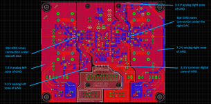
I'm making myself a DAC, just for learning purposes (and have some fun) based on the PCM2912A. While checking the datasheet for the evaluation module I noticed that the ground traces, found here in blue, are much wider, in some sections, than what they need to be. What's the purpose of that? Having a pseudo ground plane? And why the copper ground pour under the IC?
Thanks in advance!
PS: I'm not sure if this is the correct section for the post.
I noticed that the ground traces are much wider, in some sections, than what they need to be.
And why the copper ground pour under the IC?
The trace inductance is proportional to the ratio of length/width. The lower, the better.
Under the IC is a low inductance system common.
The trace inductance is proportional to the ratio of length/width.
Under the IC is a low inductance system common.
Didn't knew that! Thanks!
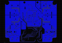
By the way, since I'll be using a two layer pcb, can I simply make a ground plane and
connect all the grounds to that or should I go down the route of star grounding?
A proper ground plane with careful parts placement should be much better than star grounding.
Use smt decoupling with short connections to keep the parasitics low.
Use smt decoupling with short connections to keep the parasitics low.
But I'll have to use vias to connect to the ground plane. Is it still preferable?
But I'll have to use vias to connect to the ground plane. Is it still preferable?
Yes, certainly. Sometimes the ground plane can be on top also.
Last edited:
Yes, certainly. Sometimes the ground plane can be on top also.
Thank you for your opinion!!

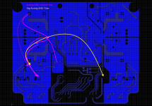
Make 2 separate pours for AGND and DGND and connect them together somewhere at the power input's capacitors .By the way, since I'll be using a two layer pcb, can I simply make a ground plane and connect all the grounds to that or should I go down the route of star grounding?
Make 2 separate pours for AGND and DGND and connect them together somewhere at the power input's capacitors .
Usually, they have to be connected at the dac chip.
To me it's an open question whether or not it's a good idea to split ground planes at all; two former colleagues of mine were very much in favour of having one and only one ground plane because they never managed to get split-ground-plane PCBs to work properly.
If you do split them, connecting them at the DAC seems to be the most logical solution. It results in the smallest detour for the return currents of signals that cross the boundary between digital and analogue.
If you do split them, connecting them at the DAC seems to be the most logical solution. It results in the smallest detour for the return currents of signals that cross the boundary between digital and analogue.
Agreed, one ground plane can be fine. However, its still probably a good idea to think about where ground currents are flowing. For example, if most of the digital circuitry is in one area of the circuit board, the ground return connection to its power supply probably should be located around there somewhere and not necessarily next to the analog ground return connection at the other end of the circuit board.
Thank you all for your replies! It has been really informative!
This leads me to my next question. Is a regular "trace connection" good enough, or should I connect the different ground traces with ferrite beads!?
Would it provide any tangible benefit!?
Thank you and merry Christmas!
This leads me to my next question. Is a regular "trace connection" good enough, or should I connect the different ground traces with ferrite beads!?
Would it provide any tangible benefit!?
Thank you and merry Christmas!
Is a regular "trace connection" good enough, or should I connect the different
ground traces with ferrite beads!?
Ground traces should always be as low impedance as possible.
Ground traces should always be as low impedance as possible.
No ferrite beads! Got it!
No beads and as short a connection as possible to the ground plane.
Thank you!
This is the must for the RF circuits onlyGround traces should always be as low impedance as possible.
[Markw4=rayma;]Agreed, one ground plane can be fine.[/Markw4]
There are may be occur additional interferences from DGND to AGND in this case
Why it (the low GND impedance) is a must for the RF circuits only? We are talking here about 22.xxxx - 49.xxxx MHz frequencies or even higher for ESS chips.This is the must for the RF circuits only
There are may be occur additional interferences from DGND to AGND in this case
That is why the star ground under the DAC chip is the best solution. The different currents will flow on the shortest way and the interferences between the different currents will be extremely low.
The star ground "ideea"should also be respected even there is a dedicated ground plane on a 4 layers PCB project.
I have got very good results with 2 layers PCB also, but I had to use 2 ground planes carefully inter-connected, one on each PCB side and a mirror placement of the DAC chips (it is a dual mono DAC project).
Attachments
I have mean what it is more relevant for RF , for 50 MHz this is much less importantWhy it (the low GND impedance) is a must for the RF circuits only?
Is it new design technique à la "star ground" by Thorp ?That is why the star ground under the DAC chip is the best solution.
Attachments
- Status
- This old topic is closed. If you want to reopen this topic, contact a moderator using the "Report Post" button.
- Home
- Source & Line
- Digital Line Level
- Ground Pours on a DAC PCB.