...you don't have too much choice about your I/V stage, given the numbers for THD+N you're targetting. Its either opampA or opampB as no discrete circuit will come close in terms of measured linearity...
That is, and has been, the case. It may be that my analog designer friend will want to try a discrete approach, I know he has been doing some thinking about it. Will have to wait and see how things turn out.
However, while measured distortion is very low, subjective sound quality is very good. It just takes a lot of work (and some expense) with SD dacs to get it right. Most designs you see around here have their little peculiarities, one might say (IMHO). Even today, people are still finding additional considerations for minimizing sources of distortion. There are no Self or Cordell books listing every possible known problem for dacs.
Last edited:
Parallelling DACs progress report
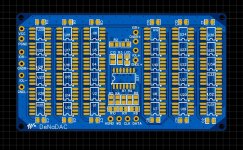
The 36 DAC prototype I featured a few posts back is now up and running. I've yet to come up with a relatively foolproof way of paralleling lots of chips so it looks like a PCB is going to be the best solution. Here's a board that's just gone out for manufacture - once I've proven it I'll share the gerbers here.
Today I've updated my Hackaday project pages with a couple of logs, if anyone's interested in some of the background thinking behind the use of a transformer in an Iout DAC then you might find these links useful : Going beyond PhiDAC | Details | Hackaday.io How a transformer helps... | Details | Hackaday.io
Attachments
Certainly it would need adjustments not simply limited to the I/V resistor.
The main reason for changes is because there are current sources involved which pre-bias the transistors to help improve the circuit linearity and set the DC operating point. The most critical is the first transistor, right after the filter - if you add more DACs this transistor deals with bigger current swings and a higher DC bias current. Therefore its input impedance will become lower and it'll need a change to its emitter degeneration resistor. This resistor's function is to pad the input transistor's Re to match the output impedance of the filter - at higher current the Re is lower and you'll need a higher degen R.
The main reason for changes is because there are current sources involved which pre-bias the transistors to help improve the circuit linearity and set the DC operating point. The most critical is the first transistor, right after the filter - if you add more DACs this transistor deals with bigger current swings and a higher DC bias current. Therefore its input impedance will become lower and it'll need a change to its emitter degeneration resistor. This resistor's function is to pad the input transistor's Re to match the output impedance of the filter - at higher current the Re is lower and you'll need a higher degen R.
Most of the stock of 1387s were intended for SoundBlaster soundcards (mid to late 1990s).The latest SAA7220 I have is '92. So I guess not much longer... They must have counted on digital filters integrated in the other ASICs, otherwise they would have accounted for NON-OS operation?
If anyone knows the schema of the SB cards, you may have your answer.
finished the I/V, works but dont think its set up quite correctly. There is only 1.5V on the output of all 4 I/Vs, I think it may be due to the LED used for bref, its some amber LEDs which I had and it doesnt light up, if it supposed to or not.
The schematic doesnt specify a type but I assume its important.
btw what is best way to support you for your work here?
The schematic doesnt specify a type but I assume its important.
btw what is best way to support you for your work here?
Yes the LEDs are all supposed to light up as they're run with forward bias of a milliamp or more. Check the voltages across all the LEDs - they're fairly critical as they set the DC bias points.
I'm not sure of your question at the end - you want to support me, financially? I don't look on what I do here as 'work' rather its fun pushing the boundaries of affordable but good-sounding DACs.
I'm not sure of your question at the end - you want to support me, financially? I don't look on what I do here as 'work' rather its fun pushing the boundaries of affordable but good-sounding DACs.
The LED was blown actually but seemed to still work, after replacing nothing changed aside from it being illuminated. There is 4.3V after the LED.
I forgot to mention I am using BC327 instead 807, I thought this was through hole equivalent of 807 but it has higher gain bandwidth product, shouldnt matter right?
Also bought ''16'' variant of the transistor with hFE from 100-250 by mistake when the ''40'' 250-600 variant is specified in V2 BOM, again dont think this should matter.
This is the Ling I/V from the link in the first post, not the V2 version, so only 1 LED.
You were offering sets of kits at one point, not sure if that offer is still open, but I guess you weren't intending to gain anything from that, only to make it easier and cheaper for others to build them?
With a 6V supply there should be about 4V on the LED if its an amber/yellow one (around 2V) - 4.3V sounds a bit too high as then the DAC's output pin is held too high. The DAC chip itself needs to run at 6V - check that its output pin isn't higher than 4.6V.
The transistors you're using seem fine.
I still have a few kits left of the original PhiDAC design. My aim of selling kits has been to encourage DIYers to build DACs themselves and make them as presents to give to others around them. This way word gets spread and also enjoyable sound is shared more widely. Once I've worked out all the fine details of the new parallel DAC design I may well do kits again to get that more widely shared.
4.8V is outside the compliance range of the DAC, it really needs to be lower. R15 (62R) can be raised in value to get this voltage down to 4.5V - try changing it to 330R.
If you'd just like a single PhiDAC kit then try contacting those who bought packs of 10 kits to see if they've got a spare one to sell. If you're not in a hurry though I'd wait for the parallel DAC kit (I plan to call it 'DeNa DAC') to show up. Its BOM cost is going to be significantly higher than PhiDAC (for a start it'll have two PCBs at least) but for a DAC it'll still be very cheap.
If you'd just like a single PhiDAC kit then try contacting those who bought packs of 10 kits to see if they've got a spare one to sell. If you're not in a hurry though I'd wait for the parallel DAC kit (I plan to call it 'DeNa DAC') to show up. Its BOM cost is going to be significantly higher than PhiDAC (for a start it'll have two PCBs at least) but for a DAC it'll still be very cheap.
yeah, that got it down to 4.5V. Seems to be working ok AFAICT, only there isnt the expected 3.9V on the output of the I/V.
I'll wait then, looking forward to hearing what a proper attempt at paralleling can do.
In theory, would this offer very low noise floor, rivalling that of the modern Sabre DACs?
Really the Sabre DACs need to operate in mono mode with all 8 outputs in parallel to achieve their advertised figures.
I'll wait then, looking forward to hearing what a proper attempt at paralleling can do.
In theory, would this offer very low noise floor, rivalling that of the modern Sabre DACs?
Really the Sabre DACs need to operate in mono mode with all 8 outputs in parallel to achieve their advertised figures.
The 3.9V figure I mentioned was because I made the assumption you were building the v2 lingDAC. For the v1 lingDAC it will be lower - I reckon it should be about 2.3V. The v1 lingDAC used more than one DAC chip (four I think) so if you're only using one that's another reason for a difference.
No, the noise floor won't get anywhere near that for the latest ESS chips. In theory the noise goes down by 3dB for doubling of the number of chips but eventually the noise gets limited by the fact of only accepting 16bits - if the recording's correctly dithered this sets the lower limit around -93dB. Driving an array of paralleled DACs can get to better than 16bit performance but it'll need an MCU to direct the different I2S streams to the various DACs - that'll probably come on a later generation 'DeNa DAC'
No, the noise floor won't get anywhere near that for the latest ESS chips. In theory the noise goes down by 3dB for doubling of the number of chips but eventually the noise gets limited by the fact of only accepting 16bits - if the recording's correctly dithered this sets the lower limit around -93dB. Driving an array of paralleled DACs can get to better than 16bit performance but it'll need an MCU to direct the different I2S streams to the various DACs - that'll probably come on a later generation 'DeNa DAC'
Had to recheck that, it turns out it is the V2 i/v, the one linked in the first post.
This was labeled as V2 (...'2V') and looked more complex which threw me off, obviously it predates the real V2.
I have seen the DAC array mentioned before, not sure anyone has actually attempted it?
Might be because of how rare/expensive most of NOS chips have become.
At that stage seperate L+R channel data would be an ''easy'' addition to the design.
I would be interested in a PhiDAC kit, and parallel kit if you decide to do it.
I have five PhiDAC kits available! The kit is free, you just pay for shipping.
I believe I mentioned above that I was out of kits. That was the case. However, someone originally contacted me for five kits, to further re-distribute in his country. But it's been a month since I've heard from him, and I never received his shipping details. So I'm putting the kits back up for grabs.
Counter-proposal
How about braxy cover ALL costs and add a couple of bucks on top for the COURTESY of a favorable review?I have five PhiDAC kits available! The kit is free, you just pay for shipping.
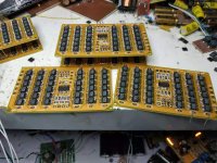
Paralled DAC progress...
The PCBs came in at the beginning of the week and I've been hunched over my soldering iron for a few hours building some up. Initially I decided to build a stack of 4 boards but that turned out to be way too ambitious to do in one leap, without prior testing of the individual PCBs. When I first powered up the 4 board stack it sounded terrible - noisy. Which means some of the DAC chips had failed, so I had to take it apart again to see which. Lesson learned - some leaps are just too great to make!
I was curious to find out if it was something I'm doing in the circuit which was causing chips to fail or if they were suspect even before I plugged them in. As I haven't figured out a way to test a chip out of circuit yet I decided to put them down on the PCB but only solder the two power pins - mainly to simplify extraction if they're proven to fail. With power on, pin7 is the experience-proven way to check if they're OK - the voltage on this pin is supposed to be 1/6th of the supply voltage (so 1V when 6V is used to power them). It turns out that it varies a little bit. maybe 10mV either way but is fairly predictable on a working DAC. But non-working DACs give voltages far away from this - from a few hundred mV up to 5V or so.
So far, having soldered in 216 DAC chips I've found about 9 to have failed. What's odd is that I can't remember prior to this having found a single dud out of the tube, though I've blown up more than one in-circuit. Something of a mystery.
Attachments
Last edited:
- Home
- Source & Line
- Digital Line Level
- lingDAC - cost effective RBCD multibit DAC design