The intention of this thread to be able to provide a High quality (low noise)VREF mainly for DACs based on the starting circuit.
(in the Thread of ES9038Q2M a discussion started for AVCC Voltage source - battery based)
In this thread I would like to discuss an OPA based circuit.
The very base circuit is not a completed one, naturally filtering capacitors, (or against oscillation), component selection, etc is in front of us)
It should be modelled and built and measured too.
If someone willing to participate feel free to comment and modify.
I have to mention that I merged 3 ideas from the following sources:
1) OPA as power supply
Frans de Wit from diyaudio:
Balanced input all DC coupled RIAA preamp (the 4th picture)
2) Walt Jung who used LED in an OPA circuit as VREF
GLED431: An Ultra Low Noise LED Reference Cell | Walt's Blog 2014
3) And JFET (2SK170) as low noise current source from the SALAS shunt circuits.
(Likely these ideas originally derives from someone else, but I have seen at these sources and though it is correct if I mention them here.)
Szabolcs (babolcs)
Attachments
Last edited:
Maybe helpful to take a careful look at this: http://www.waltjung.org/PDFs/Walts_Blog_2014_GLED431.pdf
and this: Mr. Jung's ultra-low noise VREF - the GLED431
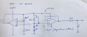
Also, for clarity I will copy the "4th picture down," as referenced in the first post by the OP. As can be seen, opamps are used directly as power supply regulators, similar to the ESS recommended opamp VCCA circuit only with 1uf output capacitance instead of 47uf (or 10uf), and a little less loop gain.
and this: Mr. Jung's ultra-low noise VREF - the GLED431
Also, for clarity I will copy the "4th picture down," as referenced in the first post by the OP. As can be seen, opamps are used directly as power supply regulators, similar to the ESS recommended opamp VCCA circuit only with 1uf output capacitance instead of 47uf (or 10uf), and a little less loop gain.
Attachments
Last edited:
Maybe helpful to take a careful look at this: http://www.waltjung.org/PDFs/Walts_Blog_2014_GLED431.pdf
and this: Mr. Jung's ultra-low noise VREF - the GLED431
Also, for clarity I will copy the "4th picture down," as referenced in the first post by the OP to this thread. As can be seen, opamps are used directly as power supply regulators, similar to the ESS recommended opamp VCCA circuit only with 1uf output capacitance instead of 47uf (or 10uf), and less loop gain.
Dear Mark, many thanks for the clarification. Yes this article from Walt was one of the starting Pont
") . I think application of OPA can have some great advantages. The PSRR is extremely high. For this model roughly 120dB. If we can manage the operation in this circuit definitely not this will be the main source of noise. The other can be the input noise, which is mainly eliminated with the OPAa output sourcing. I mean that neither the resistors nor the led is powered from the unfiltered VCC. Tomorrow evening I intend to do a test build with 5534. Sz.
. I think application of OPA can have some great advantages. The PSRR is extremely high. For this model roughly 120dB. If we can manage the operation in this circuit definitely not this will be the main source of noise. The other can be the input noise, which is mainly eliminated with the OPAa output sourcing. I mean that neither the resistors nor the led is powered from the unfiltered VCC. Tomorrow evening I intend to do a test build with 5534. Sz.Thinking about it a little more, fet or bipolar, series resistor with the transistor, all that, are not the point at all from the perspective of their noise contribution. As noise sources they are effectively in parallel with the LED and its low incremental resistance should should pretty much define noise there. They can't lower it much more at least to the extent we are talking about thermal noise. What the transistors and resistors up there around the transistor are there for is to make a simple current source. The question would then be which current source of the two offers the best regulation performance, no? Also, from Jung's perspective the B-E junction could be used to help achieve a particular output voltage.
Aside: Don't know about in this case but sometimes series elements if carefully chosen can help with temperature compensation, something that often used done with diodes and zeners. The were run at a series current where their tempcos happened to cancel out. Those were the old days, oh well.
Okay then, I provided some info about one of the resistors I asked you to think about. What about the other resistor?
Last edited:
You have some resistors in the circuit, one in series with the fet and one at the output of the 2nd opamp. How would you quantify their effects on noise?
@baboics - have you considered using an inductor rather than a resistor in the output filter/stabilizing network? It'll for sure contribute less noise than a resistor.
You could consider an older circuit that Walt also designed:
http://waltjung.org/PDFs/Build_Ultra_Low_Noise_Voltage_Reference.pdf
http://waltjung.org/PDFs/Build_Ultra_Low_Noise_Voltage_Reference.pdf
@baboics - have you considered using an inductor rather than a resistor in the output filter/stabilizing network? It'll for sure contribute less noise than a resistor.
The output resistor thermal noise definitely counts. For 50ohm it is 1nv/sqrt(Hz). For 100 it is 1.4 roughly.
Since a capacitor is used this will be devided, varying with the frequency. So a pink noise is generated by the output. Definitely an L could be better. But this R also limits the max current. Of the OPA. (At Starting it is high).
Also the input part can be lowered to a certain value. The ad797 has quite high output current. 50mA. For OPA1 the resistors +(FET +LED) +the 2nd OPA base current+ 2nd OPA output current are the load. 14+2+8 are the first three. So for output roughly 10-15mA can be calculated. It would be also possible that the 2nd OPA is a different type which operates from 2.5+2.5V. And in that case the VCC for 2nd OPA can be reduce to 7V. (Ad797 minimum is 10) but here the PSRR is decreasing and other properties too. (Can’t find diagram for the Ad797, just for LME49720)
BTW In the original circuit the BE has higher thermal effect then the FET sourced LED.
Besides these I have a big question mark referring to the whole circuit:
Will it start at all?
I modelled the DC operation in Spice and it showed normal expeted values. But if at starting time the OPA1's output is at 0V than it never will start. (this was not discussed in the original Walt article).
depends on the particularly bought OPA1's offset (positive or Negative)
But in this circuit the situation is even worth since the FET source will not work under 4V. so likely a parallel resistor/Cap is needed there. ??
I considered a pull up resistor, but it could be done only from the unfiltered VCC which would dramatically increase the noise.
Mark you were right in the ES9038 thread that it has to be bulit - Spice doens't answer all the questions.
Will it start at all?
I modelled the DC operation in Spice and it showed normal expeted values. But if at starting time the OPA1's output is at 0V than it never will start. (this was not discussed in the original Walt article).
depends on the particularly bought OPA1's offset (positive or Negative)
But in this circuit the situation is even worth since the FET source will not work under 4V. so likely a parallel resistor/Cap is needed there. ??
I considered a pull up resistor, but it could be done only from the unfiltered VCC which would dramatically increase the noise.
Mark you were right in the ES9038 thread that it has to be bulit
- Spice doens't answer all the questions.What if you have, say as one possibility, a relay operated by the output voltage of the regulator that disconnects the pullup resistor at the appropriate time? Doesn't have to be relay of course. Depends on how disconnected you would like it to be vs the downsides of relays. Part of engineering is always looking at trade-offs, right?
Of course one thing we sometimes admire about good designs is an ability to do what needs doing, yet do it with elegance. Kickers to start up a circuit sometimes may need to be tolerated, but perhaps better alternatives exist.
Also, speaking of doing what needs doing, do we know what a DAC reference needs do, numerically speaking that is? How can we know how to specify the engineering goals for this? In other words, what are the must haves and what are the nice to haves for a DAC reference. For one thing it may very greatly depending on the type of DAC.
In addition, say for an ESS DAC, There needs to be two (for stereo, perhaps more for surround) AVCC supplies to minimize channel cross-talk. However, only one reference is needed. In fact, be good if all channels used the same reference. Helps keep channel gains balanced. ESS and the power supply in the diagram number four both dispense with an output resistor and adding one could only reduce regulation at the load. Why add one in that case?
Moreover, would simply using a low-noise Jung regulator and as many buffer/followers as needed for the number of AVCC channels be more than enough for an ESS DAC? Without any effort directed towards formal analysis, my guess would be probably it would be more than enough. If so, why add unnecessary cost and complexity?
And might we not need to add a little necessary complexity if the DAC is an ES9038PRO and AVCC current requirements are more than one opamp can deliver? Can we accomplish that within the design goals? (I will stop here since we don't have design goals yet.)
Last edited:
What if you have, say as one possibility, a relay operated by the output voltage of the regulator that disconnects the pullup resistor at the appropriate time? Doesn't have to be relay of course. Depends on how disconnected you would like it to be vs the downsides of relays. Part of engineering is always looking at trade-offs, right?
Basically good idea. With a transistors+capacitor can be easily done a starting circuit which is “closed” after a certain time. I will try if it will not start. Thx
You can not put a capacitor directly on output of the OP because a stability problem.
Yes you right this is why the output resistor were considered. Inspire of its noise effect. Possibly it can be decreased.
In addition Mark raised earlier to have capacitor for OPA2 VCC. If it is needed for stability then there an R component has to be considered too. Let’s see from the tests.
At home I have some base OPA TL071 ne5534 so the base operation can be tested by me I will report hopefully in the evening.
At home I have some base OPA TL071 ne5534 so the base operation can be tested by me I will report hopefully in the evening.
You can not put a capacitor directly on output of the OP because a stability problem.
Actually, sometimes you can.
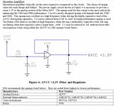
On page 4 of this application note one can see what it says about stability of an opamp and output cap with no resistor for an AVCC supply for ESS Sabre DACs: http://www.esstech.com/files/4514/4095/4306/Application_Note_Component_Selection_and_PCB_Layout.pdf
babolcs: You should have read the application note already before agreeing it can't be done. To be a good designer you have to do your homework. Right?
After seeing that it actually can be done in some cases, can either of you guys now explain how it can be possible in terms of loop gain and phase shift?
For convenience I will attach a copy of the page below.
Attachments
Last edited:
In addition Mark raised earlier to have capacitor for OPA2 VCC. If it is needed for stability then there an R component has to be considered too. Let’s see from the tests.
At home I have some base OPA TL071 ne5534 so the base operation can be tested by me I will report hopefully in the evening.
Once you figure out why a cap can be attached to the output of an opamp in the ESS AVCC circuit and not cause oscillation, you should be able to figure out it should be likely to cause oscillation in the case of the Vcc supply you mentioned.
If you can't figure it out, I will give you the answer, but you should try first. That's part of learning about design. There won't always be someone who can tell you all the answers, even today with the internet and forums, it can still happen. I will tell you this: it depends among other things on layout and types of capacitors used, information that may not be included in a schematic.
Last edited:
- Status
- This old topic is closed. If you want to reopen this topic, contact a moderator using the "Report Post" button.
- Home
- Source & Line
- Digital Line Level
- OPA based Ultra Low noise VREF for DAC