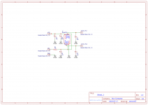
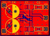
PCB (AVCC_LR)
*.json project files in zip.
Looks nice. Hope you won't be offended if I point out some potential issues, most of which we have already experienced having to sort out to improve sound quality. If I may:
ESS has specific advice about keeping AVCC on the dac ground plane and adjacent to the dac chip AVCC pins. http://www.esstech.com/files/4514/4095/4306/Application_Note_Component_Selection_and_PCB_Layout.pdf
It turns out that merely connecting a 10k and 10uf input filter to noisy 3.3v power will adversely affect dac sound quality. The AVCC input should be fed from a dedicated low noise 3.3v reference. LTC6655 or LT3042 with no other loads attached might be suitable.
Also, LME49720 is sensitive to some types of RF, such as 2GHz from DECT phone base stations. It should be shielded from RF to prevent unwanted distortion, or the dac places in an enclosed metal box. Probably better to use OPA1612 anyway, less sensitive to RF and may sound a little better too. Dual AD797 AVCC regulators might be slightly better yet, and can also be used for ES9028PRO.
In addition, another possible consideration is with the opamp VCC- connected to ground, then the opamps are running with inputs and outputs offset to within 3.3v of VCC-. Don't know if it affects sound quality, but in a non-inverting configuration, common mode distortion may be higher when the inputs are far from centered between VCC+ and VCC-. You might try connecting VCC- to -15v and see if any audible difference. That being said, the smallest audible differences won't be noticeable/audible until everything about the dac is as cleaned up as it should be.
I have seen no problems with damage to the dac by powering AVCC opamps from +-15v. If concerned about possible damage that could occur if the opamp outputs are too high or too low, zener clamps in the + direction and schottky diodes in the - direction could be used.
At some point there may also be a need to derive Vref signals from AVCC_L and AVCC_R. Recently, there has been some discussion over at ASR about eliminating the 'ESS hump' by, among other things, setting Vref to other than exactly AVCC/2. ESS THD ‘Hump’ Investigation | Page 14 | Audio Science Review (ASR) Forum
Last edited:
Thank's Mark!
This is a project witch, I believe, is enough flexible, so anyone can change parts, according specific needs.
Vref is only voltage input, so I'm sorry for misleading here...
About grounding plans...
The PSB is with strong ground (log time ago, I build many RF amplifiers) and with large traces, I hope.
Why LME49720?
I'm trying OPA2134, witch output stage is the same as OPA1612, and I'm not satisfied at all.
May be OPA1612 is OK, I don't know. But both OPA1612 and OPA2134 has a common emitter output stage. LME in other hand, has common collector, so it is better for loads like DAC AVCC, I believe. Just now, my AVCC power supply is based on LME, and sound is way better, than OPA2134. I beleive, that ADA797 or ADA4898 or any fast, low noise, low THD, high output currant OP Amp will be better. Again, I'm not tried OPA1612... yet")
P.S.
Topping D10 (ES9018K2M), has not THD Hump. Vref is not AVCC/2 here.
Vref (Topping D10) is formed - 3.3v to 10k & 4.7k to GND (1.05V).
Rin = 806ohm, RF = 910ohm.
Regards,
Ivo
This is a project witch, I believe, is enough flexible, so anyone can change parts, according specific needs.
Vref is only voltage input, so I'm sorry for misleading here...
About grounding plans...
The PSB is with strong ground (log time ago, I build many RF amplifiers) and with large traces, I hope.
Why LME49720?
I'm trying OPA2134, witch output stage is the same as OPA1612, and I'm not satisfied at all.
May be OPA1612 is OK, I don't know. But both OPA1612 and OPA2134 has a common emitter output stage. LME in other hand, has common collector, so it is better for loads like DAC AVCC, I believe. Just now, my AVCC power supply is based on LME, and sound is way better, than OPA2134. I beleive, that ADA797 or ADA4898 or any fast, low noise, low THD, high output currant OP Amp will be better. Again, I'm not tried OPA1612... yet
P.S.
Topping D10 (ES9018K2M), has not THD Hump. Vref is not AVCC/2 here.
Vref (Topping D10) is formed - 3.3v to 10k & 4.7k to GND (1.05V).
Rin = 806ohm, RF = 910ohm.
Regards,
Ivo
I'm trying OPA2134, witch output stage is the same as OPA1612, and I'm not satisfied at all.
Hi Ivo,
What don't you like about it? IME, LME49720 sounds better when first starting to work on the dac. When all the problems that can reasonably be fixed have been fixed, then OPA1612 sounds better in the dac. Therefore, that you prefer LME49720 at this point suggests that you may still have a lot of work to do getting the dac to sound better. If it is your intention to get the dac sounding as good as you can, I would suggest not to cut any corners now, or you may have to go back are redo some things later when they become the biggest bottleneck at that time.
Last edited:
Topping D10 (ES9018K2M), has not THD Hump. Vref is not AVCC/2 here.
Vref (Topping D10) is formed - 3.3v to 10k & 4.7k to GND (1.05V).
Rin = 806ohm, RF = 910ohm.
Regards,
Ivo
I believe there is revised version of topping D50 coming with 9038Q2M which solves the ''hump''.
My original topping D50 had lower Vref too, around 1V, but still has that issue.
Hi Ivo,
What don't you like about it? IME, LME49720 ...
Hi Mark!
May be I have not expressed correctly...
About AVCC: I am trying OPA2134, but sound was unnatural. Lack of middle highs, mute cymbals attack, drum attack, unnatural and mute sound. If You put sound equalizer's low's & high's freq up to the limit, You will have an idea of sound when OPA2134 is used as AVCC.
Then I swap OPA2134 to LME49720 and things goes far better.
This is an experiment with no other conditions changed, just AVCC OP Amp swap.
After that, I do some Tina Ti simulations (with some pulse load). OPA2134 oscillates, with capacitive loads. May be it's true, or not, because scope is shows nothing, but anyway, sound was not good.
About I/V stage.
After original OPA2134, witch gives me tight, flat and some how "cut off" sound, I swap it to LME49720. Minor improvements. A little bit airy and light, minor improvements in sound stage.
Then swap LME to ADA4898-2. Well, things are totally different since then. Sound become more natural... (to as much as my audio equipment allows me).
Why I said this?
I'm comparing (yes, brain is tend to forget), sound of my friend jazz band - only acoustic instruments.
These things are complicated, if we want best possible results.
It's a system with too many permutation actually...
Regards,
Ivo
P.S.
Because of impossibility to edit my previous post, here is updated version of AVCC_LR PSB project.
Attachments
Last edited:
I believe there is revised version of topping D50 coming with 9038Q2M which solves the ''hump''.
My original topping D50 had lower Vref too, around 1V, but still has that issue.
Hi laserscrape!
Which OP Amp's are used for I/V stage (Topping D50)?
Regard,
Ivo
About AVCC: I am trying OPA2134, but sound was unnatural. Lack of middle highs, mute cymbals attack, drum attack, unnatural and mute sound.
Hi Ivo,
Yes, that's sounds like it allright. It means your dac still is not right. When enough of the problems are fixed then what seems like the best sounding opamp will change, if you ever get that far with the dac. It takes a lot of work. At that point you will be able to hear that the brightness and clarity of cymbals you hear now are from added harmonic distortion. You need that now because the midrange is too muddied up with intermodulation distortion. Once all the other distortion is fixed then then try OPA1612. When that opamp sounds perfectly right, you will know you have a killer dac.
Last edited:
Is there a shortcut to test i2c connections on the arduino, mcu or dac pins?
Hi Kay,
You need some pullup resistors on the I2C bus so that normally, in the absence of I2C signals, it sits at 3.3v. Then the Arduino can pull down the bus with a fast stream of pulses when you send an I2C command.
Scopes have a trigger point which if you can set. It should be maybe 1.5v or so, somewhere about half way between 3.3v and ground. Doesn't have to be exact. When an I2C command is sent, the pulses will start in the downward voltage direction (from 3.3v going down towards ground), so if possible the trigger set for the down-arrow mode, meaning when the input drops below the trigger voltage you set, the scope start showing a sweep in time as the input voltage is changing. The horizontal axis is time and the vertical axis is input voltage. Before the I2C command is sent, the line on the scope should be visible kind of high on the screen. If you short the I2C pin you are monitoring to ground, the scope trace line should drop down to lower on the screen. Scopes usually have some trigger mode options. Auto mode means the scope will sweep and display a line even if there is no trigger event. Normal mode means the scope will only scan and display a line/trace when trigger events are present. Single mode means the scope will display the first trigger event then stop. You may have to play with the horizontal sweep rate to see the I2C pulses well. If they look too close together, speed up sweep a little. If you only see one edge of a pulse, slow down the sweep speed a little. Start with the sweep speed somewhere in the middle of its range and try lower or higher sweep speeds until you start to see trigger events.
Each time you send a I2C command a series of pulses will be sent and very soon be gone. It can help if you have someone to keep sending commands for you while you adjust the scope controls for a good view. I would suggest to try with the sweep set to normal mode.
If you don't have pullup resistors and if the arduino is not connected to the dac, you could try turning on the software pullups by setting PULLUP = 1 so you can run a test. Don't forget to set it back to 0 before you quit, otherwise you might not remember you left it set to 1. If using software enabled pullups, they will pull up close to Arduino Vcc, which for your arduino will be almost 5v instead of the 3.3v we use for the dac.
For displaying other signals on the dac, auto sweep mode is usually best at first. Then play around with the controls (and of course read all the manual on the scope you can find, if no directions, I may have them around here somewhere if I look), and pretty soon setting the scope controls will become second nature.
You didn't say if you got an 10x probe along with the scope. If so, we should talk about that.
Also, commercial scope manufacturers have some good app notes you can find on introduction to scopes and introduction to probes. The old Tektronics app notes are kind of classics in that area.
Last edited:
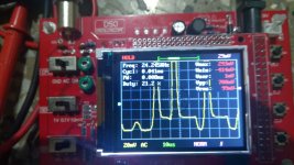
Connecting the MCU SDA pin to the red line and black to GND, I got something like the attached pic in DSO138. Does this show anything?
Hi Kay,
You should set the input coupling to DC mode for this measurement and set the vertical sensitivity to about 1v per divsion (if using a 1x probe).
Since you have the scope set to AC input coupling and 10mv per division, you are basically looking at low level noise.
Last edited:
In the above, I only turned on the dac and clipped the red to a pin under the lifted MCU sda pin, my very crude attempt at determining if the mcu still works/ if the mcu is the problem.
The MCU will need to be connected to pullups to see if it still works. You could solder leads to its lifted pins, then use some clip lead jumpers to attach pullup resistors to the wire leads so as to simulate the conditions needed for I2C bus to work. At that point you could use the scope to see if the MCU could pull down the I2C bus with clock and data pulses.
Kay,
Maybe you will find some useful info from the links below:
http://web.mit.edu/6.101/www/reference/ABCprobes_s.pdf
http://ecelabs.njit.edu/student_resources/XYZ-Scope.pdf
I2C Primer - I2C Bus
Good luck with your efforts. Hope to see you back soon.
-Mark
Maybe you will find some useful info from the links below:
http://web.mit.edu/6.101/www/reference/ABCprobes_s.pdf
http://ecelabs.njit.edu/student_resources/XYZ-Scope.pdf
I2C Primer - I2C Bus
Good luck with your efforts. Hope to see you back soon.
-Mark
Mark
after reading about the hump issue with the ESS dac, and looking at John Siau's comments, that the AVCC needs ridiculously low impedance corroborates with ESS recommendations to mount the AVCC reg close to the DAC chip. It makes sense since the current demanded by the DAC is varying at very high frequencies.
The interesting question that pops in my head is that the Voltage divider that generates Vref is generally tapped off the AVCC supply and then split with a pair of resistors. The question is whether using an independent stable voltage source not tapped off the AVCC will yield superior results or whether the modulation in the AVCC supply coinciding with the Vref modulated cancels. My thoughts are the modulation effect is not good for Vref.
What are your thoughts?
Mike,
Taking Vref from a divider is probably fine, since we use another low pass filter to clean it up after the divider. Mainly, the benefit of doing it that way is that if there is slow drift in AVCC voltage, then Vref will follow. Plus, there is not the added expense of another regulator/reference. If one wanted to, I think it would be fine to derive Vref more directly from LT6655 or whatever reference is used for AVCC, just so long as the reference doesn't get loaded down or dirtied up.
Regarding setting Vref to other than AVCC/2, it looks to me like the intent of setting it to something else is to make the quiescent output voltage of the I/V opamps = 0v. Most likely that helps reduce distortion in the differential summing stage that follows, at least that's my best guess at this point. In very basic or idealized opamp theory it shouldn't matter, but real opamps are not quite fully ideal and differential summing is kind of demanding for an opamp, at least as compared to something like a simple inverting amplifier.
The reason for using AVCC/2 for Vref in the first place is so that the dac chips analog outputs will be at 0ma when the dac is in quiescent state. That is not the same case as setting I/V outputs to 0v in the quiescent state. In fact, peak dac output currents will be asymmetrical if Vref is not equal to AVCC/2. Apparently for Sabre dacs with three opamp ouput stages, there is more to be gained by minimizing distortion in the differential summing stage than anything else (again, my tentative interpretation). Of course, it is not something ESS says anything about in their data sheets.
Interestingly, AK4499 has a voltage more or less the same thing as AVCC, except they call it the 'Reference Voltage' and it is 5v instead of 3.3v. They divide the Reference Voltage by two in order to derive a voltage level for the non-inverting inputs of their I/V opamps (same thing as setting Vref to AVCC/2 for sabre dacs). Don't know if AK4499 has less distortion with symmetrical peak output currents, and with quiescent output current = 0ma, or not. Don't know if it cares if I/V output voltages are set to 0v quiescent instead. Of course, they don't include a differential summing stage on the eval boards, so it is to the dac designer to figure out what to do. I guess we will find out at some point when people try to figure out how to minimize AK4499 overall system distortion while providing single ended outputs.
Last edited:
Have you auditioned any implementations of it?
No. I would like try test listening to something in that general vein though. Some say there is definitely better in the way of non-SD dacs, I am thinking particularly of Holo Spring dacs. However, some say they sound best with DSD1024, something it takes a very powerful computer to produce at high quality.
Otherwise, I would suggest considering an AK4499 eval board when they come out in mid-August at Digikey, if you can snatch one up. By then I should probably be able to say more about how to successfully get started with one. There will probably be no better dac for quite some time. Some of the first commercial AK4499 designs will come out without benefit of the eval board well-developed sonics to provide the dac designer some performance reference. No doubt, some of offerings will use LDOs for the critical analog supplies, and those I would tend to be wary of.
Last edited:
Just thought I would report that initial tests of USB to I2S and or reclocking boards for AK4499 eval board resulted in two of four tried having be found to work satisfactorily. They are the ones from JLsounds and diyinhk. Both of those use NDK SDA series clocks, so it may take some time before Crystek 957 clocks can be compared.
- Home
- Source & Line
- Digital Line Level
- ES9038Q2M Board