Hi Paul,Hi Mark,
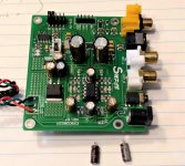
Finally done the output stage. This was my first attempt at point to point soldering and was a real challenge for me. It looks a real mess, had I known how tough it was going to be for me I would have opted to buy an output stage from Twisted Pear. But all in all it was an educational experience. I haven't tested it yet but here are some picks of the build, sure hope it doesn't go up in a puff of smoke. Because of the case I have the dac in I need to mount it directly above the dac, no room to do it any other way. I'll test it out later this week. Thanks for all of your help Mark.
Paul
Congratulations on making the output stage and thank you for posting pictures that are really helpful for me. This is my next big thing to do.
Did you had time to test it? How does it sounds?
Hiu Guys,
I just received my TP 3.3v regulators, and as I can't find no documentation, I have some questions:
-Do you know what are the 2 connectors on the left?
-Does the out & gnd on the bottom and the ones at the upper right can be used indifferently?
thank you.
Terry,
From markings on chip, we can see the TP Trident SR uses ADM7150 regulator.
Ref data sheet, page 6, pins 5 and 6 are 'ref sense' and 'ref' respectively.
Ref data sheet page 1, 'ref sense' and 'ref' are connected together and bypassed with a 1uF cap to ground.
In your pic the smd resistor is a zero ohm (marked 000) between these two pins.
So you do nothing with these connections.
You only connect to the connection points at bottom of your pic.
cheers
Terry
Thank you.
that is what I did
")
I'll test the 9038q2m with them tomorrow.
Hi Mark,
Would you please advise If I can use that particular pcb to replace CS8412 receiver which has spdif Input and output Right Justified to SM5842.
Does pcb got Input selection, for example to switch between coax and optical.
Would you please advise If I can use that particular pcb to replace CS8412 receiver which has spdif Input and output Right Justified to SM5842.
Does pcb got Input selection, for example to switch between coax and optical.
Hi bisesik,
You may need to correctly set the signal on the I2S pin header which may be called, 'DSDON,' or some other name close to that. If you are sending PCM then DSDON has to be low, IIRC.
Also, not sure if it needs the correct values for F0-F3. Could be those only matter for DSD input.
You might try reading the detailed instructions for the other, lower cost AK4137 board since it describes the signals it needs in more detail. AK4137 I2S/DSD Sample Rate Conversion Board Supports PCM/DSD Interconversion DOP | eBay
Hi Mark,
Would you please advise If I can use that particular pcb to replace CS8412 receiver which has spdif Input and output Right Justified to SM5842.
Does pcb got Input selection, for example to switch between coax and optical.
Hi samoloko,
The board I linked to for some possible help with interconnection instructions does not support SPDIF input, only I2S. It can output right justified, however.
There is another sample rate converter that does support SPDIF input and output right justified, but it is more expensive. It is this type: HIFI AK4137 DAC SRC flagship high-end audio 786K 32Bit DSD256 DSD IIS conversion | eBay
How well it might work for your application, I can't really say. It sounds like you may be trying to fix an older piece of equipment. Maybe it could be a good time to start thinking about switching to a newer dac instead of fixing an old one with an expensive part?
Last edited:
Unfortunatelly DSDON/OFF pin not helps. Anyway thank you, Mark!Hi bisesik,
You may need to correctly set the signal on the I2S pin header which may be called, 'DSDON,' or some other name close to that. If you are sending PCM then DSDON has to be low, IIRC.
Also, not sure if it needs the correct values for F0-F3. Could be those only matter for DSD input.
You might try reading the detailed instructions for the other, lower cost AK4137 board since it describes the signals it needs in more detail. AK4137 I2S/DSD Sample Rate Conversion Board Supports PCM/DSD Interconversion DOP | eBay
I wonder if it works with this board at all or not?..
Unfortunatelly DSDON/OFF pin not helps. Anyway thank you, Mark!
I wonder if it works with this board at all or not?..
It occurred to me later that the more expensive AK4137 board has two modes of operation for XMOS or Amanero that are set by holding down the selector button during boot up. They tell you not the change the clock frequency settings there or it will stop working. Also, it reads the mute pin from the little USB to I2S plugin boards. That was something I noticed when tracing out the pins that are and aren't used on the USB to I2S header socket. IIRC, maybe three or four signals come out on one side can get routed to AK4137. The other pins that are monitored go to pins on the MCU. Mute is one of those, again IIRC. Pretty sure you should be able to get that working one way or another. Especially so, if you trace out all the pins that go somewhere on the AK4137 board. I did it once out of curiosity, but didn't make a map or any other documentation for reference. It's not hard to do though. A DVM with an ohm function can be used to help, especially if it can be set to beep for continuity checks. Between looking at traces coming out from under the header socket on the top and the bottom of the board, and using a DVM to help trace them, it should be possible to make a list of all the pins that might need signals for the board to work correctly.
The same thing can be done with the low cost AK4137 board, although it uses fewer pins from the USB to I2S boards, exactly how it uses the pins it does use can be little tricky to figure out. But the same method I described for tracing out connections on the more expensive AK4137 board also works for the low cost board.
The expectation I would have is that either of the boards should be possible to get working as you want to do. Unfortunately, I don't have all the details of how to do it written down on paper for you. I guess if you don't think tracing out pins is something that will lead to a solution for you, then you could always just use the cheapest XMOS or Amanero board with two rows of pins at the end to fit the two rows of pins on the AK4137 board and it should work. The only thing I found with one XMOS board I have is that it has it SPDIF output and they used what should have been the mute pin for the SPDIF pin. I swapped them back the way they should be and wrote and post with pictures about how to do it. https://www.diyaudio.com/forums/digital-line-level/314935-es9038q2m-board-145.html#post5458654
Last edited:
Pulling the MUTE pin to GND helped a bit Now it showed me PCM 44.1kHz. Always 44.1kHz, regardless of the real SR (LRCK). But anyway it is the progress! Thank you Mark for your perseverance! 
Is it even MCLCK necessary?.. Will digging further...
BTW I know about XMOS\AMANERO and MCLK settings
Now it showed me PCM 44.1kHz. Always 44.1kHz, regardless of the real SR (LRCK). But anyway it is the progress! Thank you Mark for your perseverance! Is it even MCLCK necessary?.. Will digging further...
BTW I know about XMOS\AMANERO and MCLK settings
Last edited:
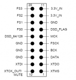
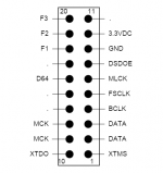
MCLK is not needed. The way the they get sample rate from the USB boards is with the F0-F3 pins. See diagrams below for Amanero pinouts. The AK4137 boards don't use all the pins, though. You would have to trace them out to see. Also, you may notice that sometimes different names are used for same signals on the same pins. The one called DSDOE is also sometimes called DSDON. Don't know why.
Attachments
Last edited:
OK, I figured it out simulataneously with you. I mean, right F0-F2 is needed to indicate the right freq. Seems that Mute is needed to reset the requesting. Well... Will try to connect this XMOS' Freq pins with F0-F2 somehow... Bad thing is that those SR indicating pins on XMOS are not isolated. BTW, DSDON/OFF is not needed. F0-F2 and Mute pins only. Even I2S! is not needed
I have spend hours trying make it work... It works now, but not as I expected. It is needed to re-pull MU-pin every time when freq is changed. If MU-pin is always on the GND, then I need to re-select USB-input to actualize freq. AUDMUTE (and DACRST too) which are on XMOS board are not help. There is "NOT LOCKED" promt until MU pin is not grounded at least for one time. I can actualizate freq manually by pulling MU to GND every time after freq of music changed. But to make it automatically "more or less" I can only by pulling MU-pin to DATA of I2S through 3kOhm. If more than 3k, then freq may not changed (depends on music). To avoid problems in SQ of music, I think that this resistor should be as much as can, because I don't want to solder any active splitter. If MU is connected to LRCK, then the freq is wrong (what "he" is doing there when showing me wrong freq ??? ), if connect to BCK\MCK - not works at all. Stupid method, but it works
I have wrong version of old XMOS pins functionality, but thanks of you Mark, you made me believe in myself
I have wrong version of old XMOS pins functionality, but thanks of you Mark, you made me believe in myself
Last edited:
In other news, finally got the clock divider board working. Figured out how to program it, and now ES9038Q2M is dead stable with DPLL set to 1. The 100MHz dac clock is divided by 4 to make 12.5MHz, a little bit high for DSD256, but it works. In particular it is outputting 12.5MHz DSD on the DSD256 setting with 16/44 PCM input from a CD rip. Don't know about that table in the AK4137 data sheet suggesting it wouldn't upsample 44.1Khz to DSD256. It works for me.
In addition to having to write bit-banging SPI code to program the divider, also found that at first the divider was outputting 75MHz instead of 12.5MHz. That turned out to be because of harmonic distortion in the LVDS inputs, which was due to no termination of the short u.fl cables. Added some 50 ohm loads at the input connectors of the clock divider board to fix that.
So far, I have only listened with headphones driven by the output stage line level output. That always adds some distortion, so I need to get the whole test setup into the test chassis and playing through the AHB2 power amp. Only then will I know how it really sounds.
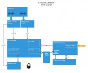
Just noticed a possibly confusing description in the last post. The 100MHz dac clock is divided by 4 to produce a 25Mhz clock signal, which replaces the 22.5MHz clock that was on the AK4137 board. That in turn, will cause AK4137 to produce 12.5MHz DSD when set to DSD256 mode. To make it a little more clear, I marked up a copy of the block diagram posted by redjr (thanks!). The 22.5MHz clock is the one the AK4137 board firmware always selects when the board is set for outputting DSD. Also, it may help to know that the 100MHz clock signal that drives the clock divider is actually output on one of the ES9038Q2M GPIO pins.
Attachments
Last edited:
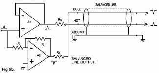
Hi Mark,
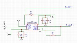
Regarding the balanced output schematic you advised, is it like the attached diagram?
Kay
Hi Kay,
Yes, that is the way shown in one schematic I posted. The inverting opamp can take its input from the output of the non-inverting opamp, or the the inputs of both inverting and non-inverting opamps can be in parallel as shown in the schematic below. When it comes right down to picking one way or the other, I guess I would probably prefer the version with the inputs in parallel, as below. That is, I would prefer it if the source impedance of whatever drives the two opamp circuits is reasonably low, such as another opamp. If the circuit could be loaded down significantly by the resistors of the inverting circuit, then that could be a problem. In that case the resistors could be made sufficiently large, or the opamps could be connected as shown on the other schematic. Since with our dacs the output impedance is usually pretty low, the parallel input circuit would probably win out.
Mark
EDIT: If you are only driving balanced lines a short distance to your power amp inputs, most likely you would not notice any difference whichever schematic version you choose.
Attachments
Last edited:
The part you mention above appears to be unobtainium. If there is an alternative you know of offhand that is available from Mouser or Digikey I might be willing to give that approach a try.
Otherwise, clock divider chips appear to be what can be reasonably obtained.
Assuming tests over the next few days show good effects on sound quality, then a low cost, easy to find and use solution that does the dividing would be probably be worth spending some time searching around for. Otherwise, some kind of circuit boards would be needed for ball-grid-array parts, or other cook-on-solder-pad parts.
Last edited:
Hi Mark,
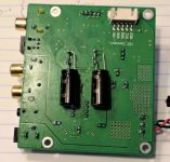
I took your advise using my DMM to check my output stage, found two mistakes that are easily fixed. In the meantime I added extra capacitance to the AVCC rails as suggested. I removed the existing 100 uF caps and put 2000uf on each rail. I had a good listen before the mod and after the mod. I have to agree that it is well worth doing, it is an easy, low risk mod that audibly increases sound quality. Sound is more liquid, the glare that can be present on high frequencies is greatly reduced, definitely sounds better. Next step straighten out the output stage and give it a whirl, need to modify my case to add some new rca outs first. Here are some pics of the cap mod, the wimpy original caps are shown in the one pic for comparison.
Paul
Attachments
- Home
- Source & Line
- Digital Line Level
- ES9038Q2M Board