Don't think I mentioned it here, but I recently wrote some tips on how to listen (or how to learn to listen) for dac sound quality. In case there is any interest in the subject, it is post #48 in the following thread: https://www.diyaudio.com/forums/dig...proving-ak4490-thd-figures-5.html#post5666915
Hi eslei,
Don't know where you got that idea, but it is not what ESS says you should use for Vref. If you would like to see for yourself, there is a schematic of an older (maybe ES9008) evaluation board schematic on the ESS downloads page. You can clearly see that Vref is taken as half of AVCC for each channel using a voltage divider as we do in our AVCC board schematic. In addition, I have the schematics for the latest ES9038PRO evaluation boards from ESS and it is still exactly the same thing.
However, I agree with you about connecting I2C on the newer 1.07 SMP CB boards in that installing J1 and J2 should stop I2C bus activity by the MCU, thus making it unnecessary to do any trace cutting or pin lifting. However, I have a 1.07 board like that here and installing J1 and J2 didn't stop it. That same board also didn't work with an optional display I got to try out with it. I assume I happened to get a board with the wrong version firmware installed. If so, it appears to be a very rare problem. Really helps to have some kind of a scope available to check such things. Also, I just kind of assumed that since Kay asked the question, he knew he didn't have one of the boards that can be stopped with J1,J2. Maybe I assumed too much?
hi, there,
as ess has the nda i don't use their information but something i can have from the internet.
if the vref is 1/2 avcc, the opamp output dc voltage wound around +1.5v not null, if that's the case? the smp cb q2m dac schematic is exactly like i record.
your 1.07 board is a coincidence, i have handled more than 20 smp cb q2m boards they all have on problem.
cheers
Hi eslei,
Right, we agree that my 1.07 board firmware issue is an oddity. It's the only one we know of like that so far.
On the issue of 1/2AVCC, there is effectively no output offset with the 3 dual opamp output stage design we use. If you are talking about the original voltage output circuit (which I think you probably are) then that would be different. When people ask me questions here about AVCC it is normally because they are modding a dac board and aren't using the voltage output stage any more. Also, the reason for using 1/2AVCC is not to set an output offset or to cancel one out, it is to minimize distortion when doing I/V conversion. Fortunately, the differential summing stage we use removes the DC offset of the I/V opamps. Another possible good thing about doing it that way is that since the I/V opamps have an offset, we can run their outputs Class A all the time by choosing the I/V feedback resistor for about a 3v p-p output swing.
Last edited:
@ Markw4
hi, there,
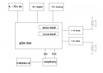
can you post a functional block diagram of your system, i wonder how the ak4137 works on your system.
cheers
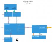
I've been following along in this thread, but have yet to start this project. In response to your query eslei and my own planning, I drafted the following diagram. This only shows the 'primary' mods that I'm aware of, realizing Mark continues with other 'minor' mods as well. I hope it's accurate enough and I will defer to Mark to point out any mis-representations, or other significant mod I missed. (I hope I got the voltages correct.)
My particular version planned is to add a RaspPi and use I2S to the reclocker in lieu of the XMOS USB board and have the audio output switchable with PRE-out. How each of these is implemented is obviously up to the individual user following Mark's more detailed instructions throughout this thread.
Attachments
redjr,
Your diagram looks pretty good. The only things I would probably add would be +5v power also going to the AK4137 board, and then three LT1763 3.3v regulators soldered onto the dac board ground plane down at the digital end for the clock, for dac chip VCCA, and for DVCC.
Maybe good to label the AK4137 as a Sample Rate Converter rather than a reclocker, too. It is a SRC and PCM<->DSD converter.
Last edited:
Hi Markw4!
As I saw you have the same AK4137 board as mine ( HIFI AK4137 DAC SRC flagship high-end audio 786K 32Bit DSD256 DSD IIS conversion | eBay )
I have a problem with indicating the stream from my USB-I2S (XMOS from DIYINHK) on the display. All other rca\opt\etc inputs are recognized OK and showed on the display: PCM\freq. I2S input works, DAC played normally. But how to force 4137 recognize stream from I2S input correctly? There is no F0-F3 outputs on my USB-I2S board, I connected LRCK\DATA\BCK only, but pulling up (to +3.3V) F0-F2 on the I2S input header according to the table not helps. Any idea? Thank you!
My USB-I2S is exactly the same: DIYINHK Isolated XMOS USB Interface | H i F i D U I N O
Hi bisesik,
You may need to correctly set the signal on the I2S pin header which may be called, 'DSDON,' or some other name close to that. If you are sending PCM then DSDON has to be low, IIRC.
Also, not sure if it needs the correct values for F0-F3. Could be those only matter for DSD input.
You might try reading the detailed instructions for the other, lower cost AK4137 board since it describes the signals it needs in more detail. AK4137 I2S/DSD Sample Rate Conversion Board Supports PCM/DSD Interconversion DOP | eBay
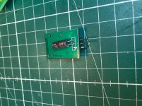
Hiu Guys,
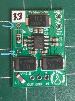
I just received my TP 3.3v regulators, and as I can't find no documentation, I have some questions:
-Do you know what are the 2 connectors on the left?
-Does the out & gnd on the bottom and the ones at the upper right can be used indifferently?
thank you.
I just received my TP 3.3v regulators, and as I can't find no documentation, I have some questions:
-Do you know what are the 2 connectors on the left?
-Does the out & gnd on the bottom and the ones at the upper right can be used indifferently?
thank you.
Attachments
Hi terry22, Twisted Pear has their one forum here:
https://www.diyaudio.com/forums/twisted-pear/
You can ask question about TP regs probably at the Buffalo topic: Introducing the Buffalo III-SE-Pro 9028/9038
There are no connections on the left side, but you can use a through hole resistor instead the original smd-one or just install a jumper over there.
Hiu Guys,
I just received my TP 3.3v regulators, and as I can't find no documentation, I have some questions:
-Do you know what are the 2 connectors on the left?
-Does the out & gnd on the bottom and the ones at the upper right can be used indifferently?
thank you.
Last edited:
Hi terry22, Twisted Pear has their one forum here:
https://www.diyaudio.com/forums/twisted-pear/
You can ask question about TP regs probably at the Buffalo topic: Introducing the Buffalo III-SE-Pro 9028/9038
There are no connections on the left side, but you can use a through hole resistor instead the original smd-one or just install a jumper over there.
thank you about the resistor stuff info, Janos.
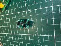
the more convenient for soldering the regulator were the 3 connections at the bottom. I added a 100uf cap as advised by Serge.
Attachments
Last edited:
Terry22,
Looks like you didn't order the TP regulator they recommend for AVCC. The one with AVCC in the name and that has two regulators on it is the one they recommend. It is also programmed for 3.6v rather than 3.3v. The higher voltage is probably okay, it is not the exact voltage recommended by ESS, but it is within the maximum limits.
Looks like you didn't order the TP regulator they recommend for AVCC. The one with AVCC in the name and that has two regulators on it is the one they recommend. It is also programmed for 3.6v rather than 3.3v. The higher voltage is probably okay, it is not the exact voltage recommended by ESS, but it is within the maximum limits.
Last edited:
Terry22,
Looks like you didn't order the TP regulator they recommend for AVCC. The one with AVCC in the name and that has two regulators on it is the one they recommend. It is also programmed for 3.6v rather than 3.3v. The higher voltage is probably okay, it is not the exact voltage recommended by ESS, but it is within the maximum limits.
Hi Mark,
Yes I know, but on TP website it is said that their avcc module is basically 2x3.3v regulators joined and boosted to 3.6v.
So, as ess recommends 3.3v, I ordered 2 regs for avvc and 1 reg for dvcc.
Do you think that it is someting better in their avcc module that makes a difference?
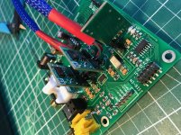
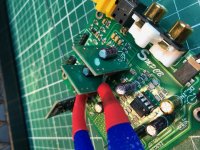
Looks like you have soldered the film caps correctly. You should probably practice cleaning up where you got some solder in places where it should not be. I would use Chem-Wik solder wick to clean up and remove excess solder.
I tried to clean the board with chem-wik, but with this board the solder really sticks strongly to the board copper and I was not able to remove it...
I will try again with a larger irin stick, but it was really difficult.
Do you think that it is someting better in their avcc module that makes a difference?
Don't know. I think they use ADM7150 regulators on the AVCC board, maybe with some extra filtering. If the same regulators on the other boards, then presumably any difference would just be the small voltage difference and maybe some extra filtering.
I tried to clean the board with chem-wik, but with this board the solder really sticks strongly to the board copper and I was not able to remove it...
I will try again with a larger irin stick, but it was really difficult.
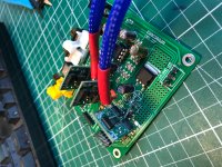
You won't be able to remove solder to leave only copper, but that's okay. The idea to remove any excess. Using some extra flux may help, as may using a larger tip and laying it down more flat on its side to make really good contact with the solder wick. If you can get most of the excess solder off, that is about as good as could be expected.
You could probably also remove some excess solder on some of the joints that look rough (cold joints, as they are called) and then add some fresh solder to replace it. Heating solder too slowly so that the flux burns out before you are done heating will also produce joints that don't look good. So-called 'cold joints' can be produced by not enough heat, or from heating too long and burning out all the flux. Either way, it can usually be fixed, by reheating if still some flux left, or by removing most with solder wick and resoldering with fresh solder. Extra flux, usually electronics paste flux can be helpful for difficult solder removal jobs.
Don't know. I think they use ADM7150 regulators on the AVCC board, maybe with some extra filtering. If the same regulators on the other boards, then presumably any difference would just be the small voltage difference and maybe some extra filtering.
They are not talking of extra filtering. If it was the case, I ordered the AVCC-SR of course. If someone has the info, tell us please.
"The AVCC-SR is essentially two Trident-SRs tuned for 3.6V output and mounted on a single board. "
Yes, I guess the important word is "essentially"..L
")
You could probably also remove some excess solder on some of the joints that look rough (cold joints, as they are called) and then add some fresh solder to replace it. Heating solder too slowly so that the flux burns out before you are done heating will also produce joints that don't look good. So-called 'cold joints' can be produced by not enough heat, or from heating too long and burning out all the flux. Either way, it can usually be fixed, by reheating if still some flux left, or by removing most with solder wick and resoldering with fresh solder. Extra flux, usually electronics paste flux can be helpful for difficult solder removal jobs.
Ok, thank you Mark about the "cold joints"
I had set the iron tip colder, cause I had read that the wima caps don't like too much heat.
And I forgot to heatup the soldering iron to make the lines after soldering the caps.
- Home
- Source & Line
- Digital Line Level
- ES9038Q2M Board