Hi Mark,
Another set of questions.
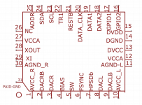
1. Am I correct in assuming that the Vref output of AVCC is to be connected to the ground (-) point of the AVCC Caps on the board?
2. Which DAC outpins pins connect to the Vref R&L input on the Output Stage Board, is it AGND L&R?
3. For the i2c connection, which one would be easier, pin-lifting or trace cutting as you have done?
Cheers,
Kay.
Another set of questions.
1. Am I correct in assuming that the Vref output of AVCC is to be connected to the ground (-) point of the AVCC Caps on the board?
2. Which DAC outpins pins connect to the Vref R&L input on the Output Stage Board, is it AGND L&R?
3. For the i2c connection, which one would be easier, pin-lifting or trace cutting as you have done?
Cheers,
Kay.
1. Am I correct in assuming that the Vref output of AVCC is to be connected to the ground (-) point of the AVCC Caps on the board?
No. The Vref for each of the left and right channels needs a wire that goes down to the the output stage board. It is connected to the non-inverting inputs of the I/V opamps for that left or right channel respectively, as should be shown on the schematic.
2. Which DAC outpins pins connect to the Vref R&L input on the Output Stage Board, is it AGND L&R?
If you look at the pinout diagram for the dac chip you can see there are two outputs for each channel. One of each has a letter 'B' suffix or other indication that it is the inverted phase output. In the output stage, all the I/V opamp circuits are inverting, so both dac outputs will be inverted there. In the next opamp, the differential summing amp, the output from one I/V is inverted again, and the other one isn't. That subtracts the two signals to take the difference. The signal that gets inverted there will have been inverted twice in the output stage, thus they cancel out and it will be un-inverted at the output. That signal should in theory come from the non-inverting dac chip output. In the schematic that MrSlim drew, he labeled the I/V inputs correctly to show which inputs should come from which dac chip outputs. Also the dac chip is arranged with outputs symmetrical about the center axis. The way I built my output stage, the outputs are also symmetrical about the center axis of the dac board. So, if the outer dac outputs are connected to the outer (or inner) I/V opamps, it all works out okay. That is to say, if the phase of the left channel is reversed, it will not hurt the sound so long as the phase of the right channel is also reversed. The most important thing is that both channels are in the same phase. I will attach the pinout diagram of the dac chip below for reference.
3. For the i2c connection, which one would be easier, pin-lifting or trace cutting as you have done?
Can't say that one is easier than the other exactly. I have always said to practice first on an old scrap circuit board before trying it on the dac board. There are a couple of risks with pin lifting. If they used a lot of hard, high temperature solder to solder down the MCU pins, then if you try to pry them off cold, chances of tearing the PCB traces may be high. If they are damaged, then you will have to solder traces to repair the connections. Also, if you bend MCU pins too many times they will break off pretty easily. Really try for bending them into place only once. If they are not perfect, but you can solder to them, then leave them as they are and solder to small leads to them, then glue the wires to the top of MCU with thick super glue or otherwise secure them against being disturbed. If there is thick, hard solder on the MCU pins, best to try to add some soft leaded solder, or maybe try to chip quik just those two pins, being careful not to get any on other pins, or you will have to clean them off and resolder them to finish the job. If you add soft solder, wick off as much as possible before trying to pry up the pins (you want the solder connection to be weak). What makes trace cutting hard is that the traces are small and close together, and jumper pins are close by making access to the traces limited. That may be the safest method since you can have some do-overs at another location on the traces if you damage them too much. The idea is to try to scrape solder mask only off the trace you want to solder. Then solder won't stick to the wrong trace. If you accidentally scrape some solder off an adjacent trace you can protect it from solder with a thin piece of mylar tape. Tin the trace first and tin the wire too, then solder them together. Again, practice first if there is any way you can find a junk board of some kind to work on.
Getting back to what happens if a pin breaks off the MCU, sometimes it may be possible to solder a tiny wire to side of the chip where some of the pin is exposed. If that doesn't work, then you would have to get to work on your Arduino to make it control the dac chip for everything. I know how to do it, so let me know if that happens and we can talk, probably offline, about what to do.
Attachments
Last edited:
Hi Mark,
I'm finishing up my output stage and will post pics soon. Just some questions to make sure that I don't screw things up. I remember you said that Vref is half of AVCC, and that I should make a voltage divider using two 10R resistors, AVCC in, two resistors on outlet, one to gnd the other is Vref. I plan on putting the dividers on my filter board to avoid hacking up the day board. Looking at the chip pinouts there is AVCC-r and AVCC-l. Can I just pull AVCC from the outlet of the regulator on the board and use the one source to make Vref-r and Vref-L. If yes can you point me to the best spot to safely pull AVCC from. If I need to pull AVCC-R and AVCC-L from the dac board could you point me to the best spots to pull them from the board.
Thanks,
Paul
Hi Paul,
The AVCC schematic (and BOM for Vref component part numbers) we use shows how to produce Vref for each of the left and right channels. It uses a voltage divider composed of two 10k 0.1% tolerance metal film resistors (not 10R!) with a 10uf filter cap to ground on the output. There is one divider for each channel to help maintain best stereo separation and the correct Vref values. You could run an AVCC wire from each channel down to the output stage board and put the voltage dividers there, or maybe put them somewhere on the dac board ground plane more towards the output stage end, wherever there is some space for them. Then from there, the Vref signals can go to the I/V non-inverting inputs for each channel. Probably good to keep the wires close to the ground plane to avoid picking up noise. A little tape can be used if it helps to keep them in place. If you are sure the wire layout is final, you could tack the wires in place with a little super glue in a few places.
Regards,
Mark
EDIT: The schematic and BOM can be found in post #3003 from MrSlim: https://www.diyaudio.com/forums/digital-line-level/314935-es9038q2m-board-301.html#post5577605
Last edited:
Hi Mark,
Great, I'll copy the divider from the AVCC schematic. Meanwhile I don't have an AVCC board yet and want to test the output stage first before moving to replace the existing AVCC on the dac board. Can you suggest a easy spot to solder wires to on the existing dac board to get AVCC-R, AVCC-L to my output stage board.
Also I was planning to feed the output stage by taking the inputs from the existing opamp holder on the dac board, any problems with that plan. I'm trying to keep my mods reversible in case I screw up.
Thanks,
Pau
1. Am I correct in assuming that the Vref output of AVCC is to be connected to the ground (-) point of the AVCC Caps on the board?
2. Which DAC outpins pins connect to the Vref R&L input on the Output Stage Board, is it AGND L&R?
3. For the i2c connection, which one would be easier, pin-lifting or trace cutting as you have done?
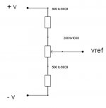
hi, there,
the vref is not related to the avcc but the opamp power supply, if that's +5v supply the +v to 5v, the -v to gnd, if that's +,- 15 v supply the +v to +15v, -v to -15v. pls see the schematic attached.
the i2c connection, what dac board do you have? if the smp cb vr1.07 we just put the j1 and j2 on will stop the mcu.
cheers
Attachments
Hi Paul,
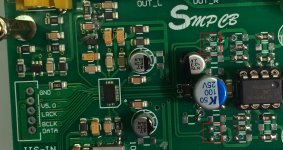
If you haven't modified the original AVCC circuit at all, you can pick up 3.3v from the bottom of the board where the existing through-hole AVCC electrolytic filter cap leads are soldered on. There is one cap for each channel. One lead of each existing cap goes to ground, and the other lead that is closer to the dac chip should be the one you want.
EDIT: While you are working in that area, you might be able to temporarily improve sound quality somewhat by tacking on some more electrolytic caps in parallel with the caps where you attach the AVCC wires. One fellow by the name of victor used three 1800uf electrolytics in parallel for each AVCC channel. He said it helped reduce harmonic distortion a lot.
Regarding where to pick up the dac chip output signals, you will need to unsolder and remove two existing SMD resistors or cut the traces leading to them from the dac chip and attach there. Probably easiest just to remove the resistors and solder your leads onto the existing solder pads (you can replace the resistors later if you really decide you want to). I drill a tiny hole between the two resistor solder pads and run a piece of #28 or #30 wire wrap wire though each hole, then solder one to each pad going to the dac chip. On the bottom of the board, twist the wires together and route them to the I/V inputs (keeping track of which wire goes to which dac output).
A pic below shows the dac output connections outlined in red.
Attachments
Last edited:
the vref is not related to the avcc but the opamp power supply...
Hi eslei,
Don't know where you got that idea, but it is not what ESS says you should use for Vref. If you would like to see for yourself, there is a schematic of an older (maybe ES9008) evaluation board schematic on the ESS downloads page. You can clearly see that Vref is taken as half of AVCC for each channel using a voltage divider as we do in our AVCC board schematic. In addition, I have the schematics for the latest ES9038PRO evaluation boards from ESS and it is still exactly the same thing.
However, I agree with you about connecting I2C on the newer 1.07 SMP CB boards in that installing J1 and J2 should stop I2C bus activity by the MCU, thus making it unnecessary to do any trace cutting or pin lifting. However, I have a 1.07 board like that here and installing J1 and J2 didn't stop it. That same board also didn't work with an optional display I got to try out with it. I assume I happened to get a board with the wrong version firmware installed. If so, it appears to be a very rare problem. Really helps to have some kind of a scope available to check such things. Also, I just kind of assumed that since Kay asked the question, he knew he didn't have one of the boards that can be stopped with J1,J2. Maybe I assumed too much?
Last edited:
A quick update on progress with the clock divider chip. A basic Arduino shield and an SPI ribbon interconnecting cable have been constructed for programming the clock divider. Code was written to send a test program to divider. The Arduino setup appears to produce correct SPI bus hardware output transitions which appear at the input connector on the clock board.
Then the next problem was discovered. The clock board has tiny SMD input voltage divider resistors which TI designed for the board with the intent of allowing the clock chip to be safely programmed by either 3.3v or 5v hardware devices. Problem is the resistor values are high enough that when combined with the clock chip input capacitance, it produces input RC LP filtering such that only very low speed SPI bus signals can work. Unfortunately, SPI is normally a pretty high speed bus (at least compared to I2C), often being clocked at several MHz. The lowest speed the Arduino SPI library can operate at is far too fast to make it past the clock board input signal LP filtering. Drat. Always something, it seems like.
Next try to will be to rearrange the Arduino program to use a much slower 'bit banging' approach to SPI signal generation. It means the existing SPI library will not be usable. This is another one of those situations where a scope is extremely helpful for seeing what is happening in a circuit. Maybe another day and then hopefully a working clock divider concept can be tested. Once basic dividing works as intended, and if minimum DPLL bandwidth is not initially achievable, then some more buttons, switches, LEDs, etc, will be added to the Arduino shield and the program modified to allow real time variations in clock divider chip settings. An interesting feature is the ability to adjust clock output phasing in relatively small steps. We'll see what happens and try to keep anyone reading along (who may be interested in the effort") ) informed as to how things are coming along.
) informed as to how things are coming along.
Then the next problem was discovered. The clock board has tiny SMD input voltage divider resistors which TI designed for the board with the intent of allowing the clock chip to be safely programmed by either 3.3v or 5v hardware devices. Problem is the resistor values are high enough that when combined with the clock chip input capacitance, it produces input RC LP filtering such that only very low speed SPI bus signals can work. Unfortunately, SPI is normally a pretty high speed bus (at least compared to I2C), often being clocked at several MHz. The lowest speed the Arduino SPI library can operate at is far too fast to make it past the clock board input signal LP filtering. Drat. Always something, it seems like.
Next try to will be to rearrange the Arduino program to use a much slower 'bit banging' approach to SPI signal generation. It means the existing SPI library will not be usable. This is another one of those situations where a scope is extremely helpful for seeing what is happening in a circuit. Maybe another day and then hopefully a working clock divider concept can be tested. Once basic dividing works as intended, and if minimum DPLL bandwidth is not initially achievable, then some more buttons, switches, LEDs, etc, will be added to the Arduino shield and the program modified to allow real time variations in clock divider chip settings. An interesting feature is the ability to adjust clock output phasing in relatively small steps. We'll see what happens and try to keep anyone reading along (who may be interested in the effort
) informed as to how things are coming along.
Last edited:
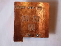
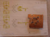
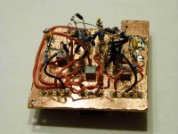
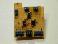
Hi Mark,
Finally done the output stage. This was my first attempt at point to point soldering and was a real challenge for me. It looks a real mess, had I known how tough it was going to be for me I would have opted to buy an output stage from Twisted Pear. But all in all it was an educational experience. I haven't tested it yet but here are some picks of the build, sure hope it doesn't go up in a puff of smoke. Because of the case I have the dac in I need to mount it directly above the dac, no room to do it any other way. I'll test it out later this week. Thanks for all of your help Mark.
Paul
Attachments
Hi Paul,
Thank you for posting pictures. I wonder if there is anyone you know who could trace out and double check all the connections to make sure wiring is okay before applying power?
Other thing is, the output stage ground plane is supposed to be part of the dac board ground plane, all in one continuous plane. From your description, you won't be able to mount it that way, but anything you can do to keep inductance low between the two ground planes would probably be a good idea. A wide flat piece of braid taken from a shielded cable might make a some kind of ground strap which would have less inductance and resistance than wire. Or maybe copper foil could be attached to cloth tape backing to make a wide ground strap. Maybe see if you can think of anything like that.
From the pictures, looks like you decided not to take my advice and do most of the wiring with very thin gauge wire wrap wire. Any reason for that? (I only suggested using larger gauge wire to the opamp power pins.)
Also, I see some resistors in the picture that don't look like .1% metal film. Are they?
If you at least have a DVM that can beep to do continuity testing, that can help to trace from the opamp socket pins back to wherever they connect to. Resistance readings can also be checked between nodes to see if they make sense.
It is good to read that despite the difficulty, you found some value in going through the experience of doing it. Most likely, you would plan things out differently if you ever did something like that again, I guessing.
In worst case, I presume you have some back up plan, like fix it if you can, else buy a TP version? I would hate to see you or any of the guys feel like giving up. I have blown stuff up before and almost always been able to fix the damage, even if it took me a couple of days. Always learn lessons to remember when something like that happens to me.
If you do have any trouble getting it to work, by all means ask before getting in too far over your head. We will try our best to help however we can.
Last of all, to all the guys who have a lot of difficulty with this through hole version, I promise that will only a little practice beforehand, SMD would be a lot easier. I know it looks scary, it scared me too before I decided to try it the first time. After the fear factor goes away, its not hard except for the super tiny things, and we either don't use any, or we have special tricks for the ones we do use.
Last edited:
Also, to any of the guys who may be new to some of this type or work, I would be happy to do a little in-person instruction/demonstration of how I do stuff. I am in Northern California, a little North of Sacramento on the way to Reno. If you are close enough to make a visit and think it might be of help, you can send me a PM and we can see what we can do.
Hi Mark,
I didn't decide not to take your advice on the wire, I forgot about it and used wire that I already had on hand. It was pretty easy to work with. All the parts were ordered from mouser using the bom listed with the schematic. The resistors on the AVCC - Vref dividers I had in my parts bin, they all measured very close with my DMM. That is a good idea to test continuity before powering up, I'll do that. I have a Twisted Pear dual mono Opus DAC that I was planning to upgrade with better power supplies (Salas) and try their discrete I/V stage (Legato). That will leave me with an extra I/V (IVYIII) so if this doesn't work I'll have a back up plan. They make nice stuff.
Also I'll dig around for some caps to put on the AVCC section of the board to see if it makes any difference. I guess I can try using some copper braid solder wick to tie the two grounds together. There are three connectors on the board that are tied to ground, I can use all three to tie to the dac ground plane. You are right about doing things differently, had I to do it again I would have made the foot print bigger, most of the problem came from trying to cram everything in such a small space. I always wanted to try a point to point build and this was an education for me.
Paul
Hi Paul,
Regarding grounds, if you make a nice, rather wide, low impedance ground strap, then no need to run ground wires too. If you do run multiple grounds, keep them all close together to avoid ground loops. The area of a loop is what makes it good at picking up stray magnetic fields, so area as small as possible is better. Also, by wide, I mean like 2" or 3" inches wide if possible. Really wide, that is. The wider the better. Run your signal wires flat against it. 1/4" wide flattened braid won't buy all that much, but is at least a little better than #24 wire or something like that. Maybe you could stick some adhesive backed copper foil to a stiff piece of paper or some cloth to make it a little less fragile, then solder it down flat at the ground planes on your boards. Seriously, whatever you can think of. We are trying to return some HF/RF junk back to the dac board and even for things like I/V signals, a ohm of ground return resistance in wire is as bad or worse than an ohm in the signal wire, since multiple ground currents will be flowing in the ground wire, something you can't prevent, and they will all cause voltage drops which may get into your amplifiers and your audio output. However, I understand you may not see things being done some of the ways I recommend here in the TP system you have. Maybe I could say this: I think the ways I recommend should be used for the projects you find here. Projects from other places are not things I want to (or should) get involved with unless invited. (OTOH, Allo Katana is an exception and something different since I agreed to be a reviewer.)
Regarding grounds, if you make a nice, rather wide, low impedance ground strap, then no need to run ground wires too. If you do run multiple grounds, keep them all close together to avoid ground loops. The area of a loop is what makes it good at picking up stray magnetic fields, so area as small as possible is better. Also, by wide, I mean like 2" or 3" inches wide if possible. Really wide, that is. The wider the better. Run your signal wires flat against it. 1/4" wide flattened braid won't buy all that much, but is at least a little better than #24 wire or something like that. Maybe you could stick some adhesive backed copper foil to a stiff piece of paper or some cloth to make it a little less fragile, then solder it down flat at the ground planes on your boards. Seriously, whatever you can think of. We are trying to return some HF/RF junk back to the dac board and even for things like I/V signals, a ohm of ground return resistance in wire is as bad or worse than an ohm in the signal wire, since multiple ground currents will be flowing in the ground wire, something you can't prevent, and they will all cause voltage drops which may get into your amplifiers and your audio output. However, I understand you may not see things being done some of the ways I recommend here in the TP system you have. Maybe I could say this: I think the ways I recommend should be used for the projects you find here. Projects from other places are not things I want to (or should) get involved with unless invited. (OTOH, Allo Katana is an exception and something different since I agreed to be a reviewer.)
Last edited:
Hi Mark & eslei,
Mark, thanks for the clarification, so one would just connect the avcc l & r.
@eslei, mine is the old blue board which does not have any i2c connection points.
I guess I'll try the trace cutting method soon as my prototype boards arrive. Hope that works.
By the way, has anybody has done the output stage with balanced outputs? If the schematic is there, I'd like to try one in the future since my amp has balanced input.
Cheers,
Kay
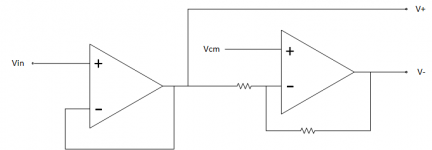
For balanced outputs, the best and most correct way is use the normal single-ended outputs as shown on our output stage schematic, then balance that signal using two dual-opamps, one per channel. Or you could use a transformer instead, one per channel. Thing about transformers is they will add some distortion.
Typical opamp balancing circuit schematic attached below. You would use one dual opamp for each channel. As always, the opamps should have decoupling caps at their power pins. If you want to use this method, just leave some extra room on your output stage perfboard to add the two extra opamps. The exact resistor values for the inverting opamp are not critical just so long as they are the same. Around 5k ohms might be reasonable. (Vcm on the schematic in this case would be ground.)
EDIT: regarding trace cutting method, I use a small jeweler's screwdriver with a sharp, unworn tip to scrape off the solder mask. I don't put the scraped off places too close to each other to avoid possible accidental solder bridges. I would suggest using a short length, tiny diameter solder iron tip, and adjust the temperature to only a little higher than enough to melt the solder. Once you tin an exposed trace and a small #30 wire wrap wire with a low temperature iron, there should still be enough flux on them to solder one more time without adding more solder. You can add a little paste flux if needed. Tape the wire in place right where you want it with gaffer tape or electrical tape, and you should kind of barely have to brush along it with the freshly-tinned solder iron tip to melt the solder used for tinning and complete the joint. If needed a tiny bit of extra solder could be added but probably not needed. Use 0.3mm diameter 63/37 leaded solder if you can find it. Its good to buy a spool of that anyway since it is highly useful for small and delicate solder jobs.
Attachments
Last edited:
I'm thinking divide 100MHz by 4 to get 25MHz. Already have an Arduino program up and running to write SPI. Need to wire it up and test it. Also, thinking about seeing if phasing the AK4137 clock relative to the Q2M clock can help optimize stable DPLL (its easy to do with the divider chip, so may as well see if it can do anything useful). Divider is LMK01000. Numbers like 30fs additive jitter from 100Hz to 20MHz sound pretty good to me. You have something better?
2 Flip Flops is all you need.
https://www.electronics-tutorials.ws/counter/count_1.html
http://www.potatosemi.com/potatosemiweb/datasheet/PO74G74A.pdf
Another option is LT6954 family. Super low phase noise, also has the LVDS OP
https://www.analog.com/media/en/technical-documentation/data-sheets/6954f.pdf
cheers
Terry
Hi Terry,
The LT6954 looks interesting. However, I'm almost at the point of being able to test the chip I have. Either way, if it works and if it needs a divider chip for best performance, a little board will have to made to solder the chip to.
Regarding flip-flops, yeah, I know. But not what I want to use for this test. If the test works, then I would be inclined to test flip-flops to see if they can work just as well for our purposes. If so, it would be cheaper and easier.
Say, you know if you would mod one of the boards along with us, then you could help run tests on some of these things. That would probably be the most useful thing you could do, and you would end up with a very nice dac, too.
Thanks for looking up the part numbers.
Cheers,
Mark
Thanks Mark, as always.
You are very welcome, of course.
Also, please post some pics for us when you can. We would very much appreciate it. It was good of Paul to post his, and I hope that can give other folks the courage or whatever it is they may need to be willing to share with the group.
- Home
- Source & Line
- Digital Line Level
- ES9038Q2M Board