Been thinking some more about I2C. We need to have a way to get in there and make some adjustments at the register level. So far no word from occip, but I have done some reading on mulit-master I2C for Arduinos and it doesn't look too good. In general, multi-master seems work best when the bus masters are signaling each other outside of the I2C bus signals so as to avoid collisions when both try to control the bus at once. That being the case, the best solution is probably a hardware one that can somehow be equivalent to pin lifting, but without the risks of bricking the dac MCU.
First though, I would say the bricking a dac MCU would not be a very big deal if there was no display and remote controls to worry about. For boards that don't have those things, an Arduino could easily control volume and or select inputs and filters, exactly what the MCU normally does. An Arduino could run the display and act as a optical remote receiver too, but it would be more work involved. There is however existing code that can used for common functions like that.
Anyway, let's say pin lifting is not going to happen so what else can we do, and if we make a mistake can we have do-overs without excessive risk of bricking anything?
I think we should be able to do meet those requirements. We can cut traces between the dac chip and the MCU and attach wires there. 30-gauge wire wrap wire would be doable, as would any smaller wire. The traces look pretty close together, but if we ruin a short section we can always trim it back a bit more and try again.
How do we keep from getting solder bridges to adjacent wires? So long as we leave the solder mask on them solder won't stick. If we accidentally scratch off some solder mask, we can cover traces we don't want to solder with thin high temperature Mylar tape so solder won't stick.
Easy to do, but the wires will be a little delicate and could get damaged later. What about that? Probably if we strain relief the area where the wires attach to the traces there won't be any damage to traces from accidentally snagged wires or something of that nature.
So my question would be, if I can make good instructions with good pictures showing how to do it in such a way so that if it gets flubbed on the first try you can have a few chances for do-overs, would that be sufficient to make you feel comfortable enough to try it?
Last edited:
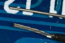
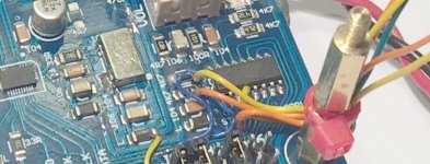
For some more ideas about tapping into the I2C traces rather than pin lifting, some pics below show the ends of a 30 gauge wire wrap wire and 32 gauge stranded wire next to the traces.
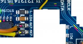
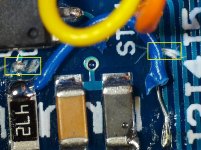
The other pic shows the SCL clock trace in yellow (excluding the diagonal yellow wire at the top of the picture which is clock power), and the SDA data trace in red/orange. Next to them is the reset trace in green.
We would just cut the SCL and SDA I2C traces going to the MCU on the Q2M side of the MCU, and on the pullup resistor side, and then solder some leads with connectors onto the traces going to the MCU pins.
The the SCL and SDA traces going to the Q2M would patched over to the pullup resistors.
Then it would be just the same electrically as if we had done pin lifting.
The good thing about it is that the traces are long enough that there could be lots of tries before running out of trace, which should never happen.
What do you guys think, could you do it?
If yes, then I will go ahead and do it, and take pictures.
Otherwise, I would be happy to accept ideas as to how we could work through or work around somehow whatever remaining concerns there may be.
Attachments
In the never ending (it seems like) quest to figure out how to lift pins or do the equivalent, I ordered some tools to try in order to see if they can make the process more reliable and less worrisome. The tools are intended to help with unsoldering ball grid ICs.
The idea would be to heat up one or more pins to soften or completely melt the solder, then use a tool to hook or slip under the one pin or few pins that are to be lifted. The other pins shouldn't move when the solder is melted so long as they are not under mechanical pressure to move.
Here is what the tools look like: Amazon.com: VIPFIX 22 In 1 BGA IC Chip Remover Tool A8 A9 A10 CPU Remover Burin Tool with Blade Set for iPhone CPU NAND Repair: Cell Phones & Accessories
If anyone else knows of similar tools please tell us about them.
Hey occip,
Question for you please. Apparently the Arduino I2C library I have been using does not support multi-mastering so it only tells me the bus is busy rather than waiting for a chance to seize it. Could you tell us what hardware/software you are using for I2C access to ES9038Q2M board dac chip?
Thanks!
Hi,
I'm using esp32 with arduino programming and the wire library
Multi mastering is not required here, as there are tiny burst of data with large period without activity. I've managed to read all the register between two data burst. If you want something more reliable, you have to monitor the clk pin and wait until there is no activity on the clk gpio, then you will be able to send a lot of i2c requests without any problem.
Hey terry22,
You are someone who has expressed interesting in building, but also concern about things that may be too difficult. Do you have any thoughts one way or the other as to your ability to solder wire wrap wire onto traces when adjacent traces are protected with solder mask and or Mylar tape? It's not hard or risky, I don't think. But, that's me.
I ask because I am starting to have a feeling that the method occip used for I2C might not be the most desirable in some respects, although he did get it to work to his apparent satisfaction.
I am willing to see what I can figure out about how much time there is between MCU messages and how many tries might be needed to adjust H2 and H3, DPLL BW, and or anything else. I would like that to be a good, non-frustrating experience when the time comes, but the best way to make it completely predictable would be if we could break the I2C connection between MCU and Q2M. Pin lifting is one way, and trace cutting/soldering seems like a much less risky one. Certainly less risky some of the other things we do when we get in there and start modding a board.
So, can I get a some feedback from you or anyone else who would like to respond as to whether soldering a little wire on could be done comfortably?
Or, would you feel better deciding after seeing some pictures of me doing it first?
We could do it that way too.
But, if there are too many self-doubts to try it, I guess I will have to put in more effort with trying to work around MCU programming, which I have always thought to be running in a tight loop without much in the way of holes. Maybe I missed some holes but I don't know what for or why they wouldn't just loop it continuously, and so I have a feeling there could be multiple tries and some resulting frustration if we go that way when we don't really need to.
Last edited:
I am willing to see what I can figure out about how much time there is between MCU messages and how many tries might be needed to adjust H2 and H3, DPLL BW, and or anything else. I would like that to be a good, non-frustrating experience when the time comes, but the best way to make it completely predictable would be if we could break the I2C connection between MCU and Q2M. Pin lifting is one way, and trace cutting/soldering seems like a much less risky one. Certainly less risky some of the other things we do when we get in there and start modding a board.
So, can I get a some feedback from you or anyone else who would like to respond as to whether soldering a little wire on could be done comfortably?
Or, would you feel better deciding after seeing some pictures of me doing it first?
We could do it that way too.
following your advice with a logic analyzer, i can confirm that we can disable the on board mcu by putting j1, j2 on, the dac ' sda ' and ' scl ' connection are ready to receive i2c command from raspberry pin 3 and pin 5. using ' I2C-tools ' on ssh is capable to configure the 90x8.
anyone who would discuss this more pls pm me, we may start another thread.
cheers
eslei,
Thank you for figuring that out. May I ask which version of the board you are using?
This time around I happen to be using one of the blue boards and not sure if the firmware is the same in it as what you have. Also, don't know if firmware is different in different versions of the green boards since some have displays and some don't.
If the J1, J2 setting works for all boards that would be terrific. Don't know if we will get that lucky or not. I will check the blue board in the morning and post results for it.
One more thing I should mention about connecting to the dac via I2C bus:
The dac should be powered on before connecting a powered-on I2C master device. That is for the usual reason that we don't want to put voltage on the input pins of a device when the power is off or it may cause damage. To some extent the pull up resistors on the dac board might help protect it by draining off some current if a high impedance source. Open collector outputs should be safe to connect so long as the only pull up resistors are the ones on the dac board.
Also, so long as the dac board is powered on, the I2C pins are rated as 5v tolerant, so it should okay to use a 5v I2C master.
Also, if any concerns it should be possible to help protect input pins against potential accidents by connecting schottky diodes from the I2C inputs to the 3.3v power bus on other side of the pull up resistors. Rectifier diodes may be good for that because you want ones with Vf as low as possible.
Last edited:
May I ask which version of the board you are using?
the green smp es9038q2m v1.07, es9028q2m v1.01 make by ustart audio.
i just have a breakthrough, volumio v2.457 hardware volume control via raspberry i2c bus is achievable now.
cheers
Attachments
Hi eslei,
Looks like you posted two pictures of smpes v1.07, one of them with AVCC and VCCA power connections outlined. Is that what you intended?
Also, I think it would be okay for you to tell us how you configured your RPi to work with the dac board so far. I think it is relevant to the thread and would be on topic.
Last edited:
Just one thing I tried and can confirm its function is Raspberry Pi + Hifiberry DAC+pro HAT with its own master clocked I2S output. This outputs connected to I2S input (only GND, BCKL, LRCLK, DATA) of the es9038q2m board works well and drivers of each SW for this DAC HAT can be used.
This Setup has 2 advantages compared to I2S Output from RaspberyPi GPIO:
1) the signal is of much better quality regarding jitter as the HAT is the master clock with its own clocks and not the Pi with its jittery on board clock
2) most SW has drivers for this DAC as sometimes it is a problem to get the raw RasPi working in just streaming I2S without any HAT on it.
It appears that blue board microcontroller I2C clock signals operate more or less continuously regardless of J1, J2 jumper settings. There are some pretty short gaps that occur periodically and independent of jumper settings, but they are only maybe 280us long.
Therefore, I will plan to do PCB trace mods on this one instead of pin lifting. Maybe it will look more appealing than pin lifting for any blue board modders.
Therefore, I will plan to do PCB trace mods on this one instead of pin lifting. Maybe it will look more appealing than pin lifting for any blue board modders.
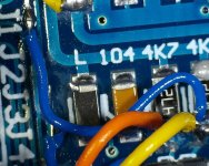
The trace cutting and I2C patching has been completed for the blue board. Where the cuts in the traces where made are outlined in yellow in one of the pictures below. Also, easy to see where I over-heated insulation on one wire when soldering it. Oh well, I will try to be more careful next time and set the iron temperature at the lowest temperature that allows soldering reasonably well. Reason the iron was set as hot as it was, was to melt the lead-free solder on the board. Too hot for that particular insulation though.
The wiring rings out okay, so the board will go back in the test system to see how much harmonic compensation it needs. Guess would be that it probably needs more than the first modded dac since the .1% metal film resistors this time aren't as good as some of the .01% thin film resistors I was able to use last time. If it turns out I guessed right, that might be a reason to consider using thin film resistors mounted on SurfBoards or some similar arrangement when building a nominally through-hole-component version of the dac mods. After all, Surfboards are through hole components")
Also, changing the subject a bit, the big size film caps arrived. They will be used find out if they can improve sound quality audibly vs using some kind of electrolytic caps for AVCC opamp output filters. The existing aluminum polymer caps are 47uf. ESS says if using LME49720 opamps, 10uf should be okay, but so is 47uf.
The film caps I have are 10uf, 22uf, and 33uf. Of course, they are physically fairly big, but there is room on top of the board where the old output stage used to be.
Initial testing will be with the existing 47uf aluminum polymer caps. Then we will see if film can help at all.
The wiring rings out okay, so the board will go back in the test system to see how much harmonic compensation it needs. Guess would be that it probably needs more than the first modded dac since the .1% metal film resistors this time aren't as good as some of the .01% thin film resistors I was able to use last time. If it turns out I guessed right, that might be a reason to consider using thin film resistors mounted on SurfBoards or some similar arrangement when building a nominally through-hole-component version of the dac mods. After all, Surfboards are through hole components
Also, changing the subject a bit, the big size film caps arrived. They will be used find out if they can improve sound quality audibly vs using some kind of electrolytic caps for AVCC opamp output filters. The existing aluminum polymer caps are 47uf. ESS says if using LME49720 opamps, 10uf should be okay, but so is 47uf.
The film caps I have are 10uf, 22uf, and 33uf. Of course, they are physically fairly big, but there is room on top of the board where the old output stage used to be.
Initial testing will be with the existing 47uf aluminum polymer caps. Then we will see if film can help at all.
Attachments
Seem to have run into a very worrisome snag here. Hooked up everything to start checking HD compensation, but thought the audio sounded a bit more scratchy and distorted than it should at this point.
Back when I installed the clock, I put it on its own voltage regulator which is the same as I did for the 1st board. However, on the first board I also put VCCA on its own regulator and I decided to see how this one sounded before doing the same on it.
Well, based on the sound quality as described above, I decided to go ahead and do it now. So, I cut the trace to the VCCA filter inductor to separate it from the dac board 3.3v bus. Checked with a meter to make sure it was cut all the way through, but it still showed as connected at about 4.7 ohms.
Troubleshooting a bit, I cut the trace just before VCCA goes to the dac chip pin. Turns out the short is either where it is soldered to the board or inside the dac chip. Not good. I will try wicking the solder off the pins in that area and see if any change. If not, then the dac chip/board may be bad.
That could cause a significant delay to my project. Don't know yet. In the worst case, we are about at the end anyway, so shouldn't hold anyone else up. More later as I know more.
So much for that dac.
So you think the DAC chip itself is toast? Bummer..
Hi eslei,
Looks like you posted two pictures of smpes v1.07, one of them with AVCC and VCCA power connections outlined. Is that what you intended?
Also, I think it would be okay for you to tell us how you configured your RPi to work with the dac board so far. I think it is relevant to the thread and would be on topic.
@Markw4
es9028q2m v1.01 on left is avcc and vcca power connections outlined.
es9028q2m driver have a look this:
ES9028Q2M driver for Raspbian based distro
and this:
GitHub - VinnyLorrin/ES9028Q2M-Linux-Driver
it works for es9038q2m hardware volume as well.
- Home
- Source & Line
- Digital Line Level
- ES9038Q2M Board