On another topic, regarding creating build instructions in PDF format, it looks like Serge may have used the 'print to PDF' function. If so, it drastically reduces picture resolution, making them almost unusable. Not sure if there is a way to make a PDF with full res pics or not. If not, then I would say PDF would be a poor choice for what we are doing here.
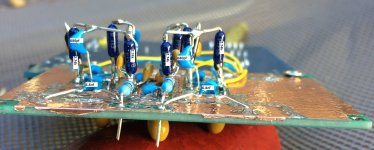
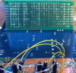
EDIT: Is the pic below helpful? 220 ohm output resistors are in red boxes. Some other components for the differential stage are labeled.
In addition, the little blue caps down against the board are ceramic power filter caps, and the little yellow ones are 220pf, or 330pf. The ones on the I/V resistors are 330pf. The others are the 220pf yellow ones. The slightly bigger blue caps more up in the air are 6.8nf or 680pf.
Attachments
Last edited:
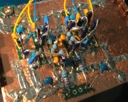
While I am trying out picture markups out, attached is some more in that vein.
The one with some colored lines on it is showing as follows:
Green shows the top of the I/V resistors that have the 330pf I/V caps soldered to them. The long bare end of the I/V resistor goes to the opamp outputs. The short end with the cap on it goes to the inverting input.
Red shows the two nodes, one for each channel, that are where multiple components come together up in the air, not at an opamp pin. The Red such nodes are associated with the non-inverting differential opamp inputs.
Light Purple is like red, except it shows the nodes associated with the inverting differential opamp inputs.
Orange denotes the output resistors and caps.
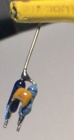
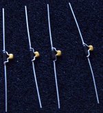
I will also attach a couple of pictures that show parts soldered together prior to attaching them to the board. Some are the I/V resistors and caps that you can see in the board pictures, and the others consist of two resistors and one cap that you can see attached to the differential opamp pins in the board pics.
This probably all gets a lot easier to make sense out of when physical components are in-hand and can be compared to what is in the pics in order to know what is what.
The one with some colored lines on it is showing as follows:
Green shows the top of the I/V resistors that have the 330pf I/V caps soldered to them. The long bare end of the I/V resistor goes to the opamp outputs. The short end with the cap on it goes to the inverting input.
Red shows the two nodes, one for each channel, that are where multiple components come together up in the air, not at an opamp pin. The Red such nodes are associated with the non-inverting differential opamp inputs.
Light Purple is like red, except it shows the nodes associated with the inverting differential opamp inputs.
Orange denotes the output resistors and caps.
I will also attach a couple of pictures that show parts soldered together prior to attaching them to the board. Some are the I/V resistors and caps that you can see in the board pictures, and the others consist of two resistors and one cap that you can see attached to the differential opamp pins in the board pics.
This probably all gets a lot easier to make sense out of when physical components are in-hand and can be compared to what is in the pics in order to know what is what.
Attachments

Last edited:
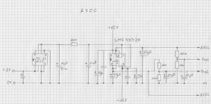
Here is the diagram of AVCC.
The 2nd cap of the decoupling is 0.1uf?
Attachments
Standard opamp decoupling caps we use are 10uf Tantalum in parallel with .1uf X7R ceramic.
For the input cap to LTC665, they say >= 0.1uf ceramic. I have been using 1.0uf ceramic because I have them and they meet the specification. Either way would probably be fine.
Decoupling caps should always be located as close to the pin as possible with short as possible leads, and connected the ground plane nearby with the shortest possible lead. Too much lead length and thus inductance makes the caps less effective at high frequencies and can also result in significant self-resonance, something we definitely don't want to have be a problem. (That's more or less my standard sort of lecture on decoupling caps.)
By the way, thank you for the drawing.") As a possible hint (if that is okay), I usually try to point opamps in the direction of signal flow. In schematics we usually show signal flow from left to right when possible. Thus, I usually show opamps with the little triangle's outputs pointed to the right. That often simplifies the look of a drawing. Same sort of idea for layouts, point the opamps in the direction of signal flow so we don't have input and output wires crossing, if possible.
As a possible hint (if that is okay), I usually try to point opamps in the direction of signal flow. In schematics we usually show signal flow from left to right when possible. Thus, I usually show opamps with the little triangle's outputs pointed to the right. That often simplifies the look of a drawing. Same sort of idea for layouts, point the opamps in the direction of signal flow so we don't have input and output wires crossing, if possible.
For the input cap to LTC665, they say >= 0.1uf ceramic. I have been using 1.0uf ceramic because I have them and they meet the specification. Either way would probably be fine.
Decoupling caps should always be located as close to the pin as possible with short as possible leads, and connected the ground plane nearby with the shortest possible lead. Too much lead length and thus inductance makes the caps less effective at high frequencies and can also result in significant self-resonance, something we definitely don't want to have be a problem. (That's more or less my standard sort of lecture on decoupling caps.)
By the way, thank you for the drawing.
As a possible hint (if that is okay), I usually try to point opamps in the direction of signal flow. In schematics we usually show signal flow from left to right when possible. Thus, I usually show opamps with the little triangle's outputs pointed to the right. That often simplifies the look of a drawing. Same sort of idea for layouts, point the opamps in the direction of signal flow so we don't have input and output wires crossing, if possible.
Last edited:
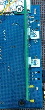
With respect to the AVCC board, it might be a good idea to go ahead and work in getting its mounting worked out before going too far with the output stage board. There is some mechanical work to do, removing the RCA and 1/8" phone jacks to make room. Some pics below showing how mine is mounted.
There is a red line border in one of the pictures showing maybe about how far the AVCC ground plane needs to come out to attach to the DAC board ground plane. Maybe it could extend a little more towards the digital end of the DAC board too.
Thing is, the DAC board has a divided ground plane (for the now relocated analog outputs) that no longer should be divided with this mod. Therefore will solder copper foil across the boundary to make one continuous DAC ground plane in that area.
Attachments
Last edited:
After looking at the AVCC board as mounted for awhile and thinking about it some more, I think I would like to revise that to move the AVCC board in a bit more towards the center of the dac board and change the mounting hardware some too.
I will try to post some new pictures later, and then let's see how it looks at that point.
I will try to post some new pictures later, and then let's see how it looks at that point.
Last edited:
Hi Serge,
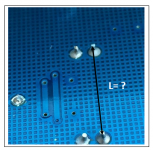
Space between the AVCC cap leads is about 13.5 mm. Center to center distance looks a little more like 14.5 mm. You asked for the distance between the caps, but your black arrow tips in the picture look more like inside to outside, which would be the same as center to center.
By the way, nice, very clear, in-focus picture you have there of the bottom of a dac board.
Last edited:
Hi Serge,
Space between the AVCC cap leads is about 13.5 mm. Center to center distance looks a little more like 14.5 mm. You asked for the distance between the caps, but your black arrow tips in the picture look more like inside to outside, which would be the same as center to center.
Thanks Mark
Center to center is good :14.5mm
Serge
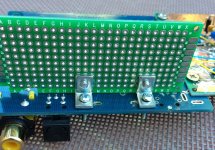
After thinking about it some more, think there is another approach to locating the AVCC board that I like better. Some good things are that it would be closer to the load and closer to power, and it would not be necessary to remove RCA analog output connectors. The less good part is that it would probably have to be glued in place rather than screwed down, and it would redistribute some existing ground current paths to some extent (although not enough to cause problems, I don't expect).
In the picture below, the red rectangular area is where the ground planes would attach. AVCC, 5v return, and +-15v return current from the AVCC board would all come out there. Likely attach both sides of the AVCC board to the DAC board ground plane. Among other things it would probably help keep it standing up. Also, the ground plane attachment on the back side from this view could be maybe a little bit wider than the red rectangle on this side. That might have the effect of diverting HF ground currents coming back from the far end of the dac board a little bit more away from the AVCC cap ground area (since we would like to keep that pristine analog power as clean as possible.
Also, some 'epoxy putty' type material could be used in the corners to also help keep it in place, roughly where the blue circles are. The good old green epoxy putty is the kind I like best for this type of use. It has an excellent track record over many years. Kneadatite Blue/yellow Epoxy Putty Tape 36 Green Stuff Toys and Games | eBay One roll of it is good for many uses too, as it keeps pretty well in storage, IME.
One implication of locating the AVCC board in this way is that it would probably be best if almost fully constructed while unattached to the DAC board, then when ready, soldered and glued in place, with =5v and +-15 as needed connected up at that time.
Still not sure where I am going to put that relatively huge 10uf film cap, which may very well be overkill, but what the heck, may as well try it out I guess.
Presumably, this looks better to everyone else out there too? Please let me know if any comments or concerns.
Attachments
Last edited:
As a possible hint (if that is okay), I usually try to point opamps in the direction of signal flow.
Thanx for the hint, I would normaly do with the correct drawing of an opamp. But in this case I did it for the better arangement of the circuits. For me I have a better orientation and I use the schema to mark cross out, witch component is done.
For the LTC6655 is it a must for the 0.025 ppm (out of stock) or is the 0.05 type okay?
Hans-Peter
The 0.05 type should be fine.
Also, I did not mean to imply that the drawing was incorrect in any way. Thanks again for working on it. Any kind of team effort is much appreciated. Unfortunately, none of us know each other personally, or know each other's experience with electronics. Also, when I write in the forum sometimes it is directed at trying to provide some information for people who may be reading along, some of whom may be just starting out.
Also, I did not mean to imply that the drawing was incorrect in any way. Thanks again for working on it. Any kind of team effort is much appreciated. Unfortunately, none of us know each other personally, or know each other's experience with electronics. Also, when I write in the forum sometimes it is directed at trying to provide some information for people who may be reading along, some of whom may be just starting out.
Last edited:
Here is the BOM with the Mouser numbers. The DigiKey will follow. There are three tabs in the sheed. AVCC, i/v and both combined.
Nice work, thank you. Just one thing, since you are a little bit ahead of me we didn't get to talk about the 47uf cap yet. I will use aluminum organic polymer or just plain aluminum electrolytic for that one. Tantalum may be more noisy than we would prefer for that application.
The argument in favor of organic polymer is the very low ESR, and that is what I used in the first dac board. The downside is they are leaky, don't know about noise mechanisms in them. Aluminum electrolytic is typically higher ESR, although there are some made that are better in that respect (I think).
The good news is both types are cheap. Easy to try either one.
Last edited:
Looks like there may be trouble ahead buying dacs and other audio equipment from China and importing it into the US without paying someone paying for tariffs.
Here is says heading 8519 is sound recording or reproduction apparatus:
Sound recording or reproducing apparatus
And it says, "8522.90.65 Parts and accessories of apparatus of headings 8519 to 8521, nesoi, printed circuit assemblies," here: https://ustr.gov/sites/default/files/301/2018-0026 China FRN 7-10-2018_0.pdf
So, presumably that may be in fact be the reason my most recent Chinese dac order was rejected by customs, just don't know. Lots of other items on that list too.
Oh well, nothing to do about that here but wait and see what happens, if it is in fact a more general problem.
Last edited:
Yet another ES9038Q2M board too: Upgraded version of ES9038Q2M decoder board I2S input OPA1612+AD8397ADRZ | eBay
Yet another ES9038Q2M board too: Upgraded version of ES9038Q2M decoder board I2S input OPA1612+AD8397ADRZ | eBay
Not much info on it yet... wonder what the switches are for ?
- Home
- Source & Line
- Digital Line Level
- ES9038Q2M Board