Hello Markw4,
I understood madds1 circuit as an easy to apply i/v output which sets the DAC to current mode. But if I understand correctly, this above circuit in my post #697 does not include the LP filter and is just i/v and single-end "transformer" and so it cannot be used as direct connection to my DAC outputs -/+?
I understood madds1 circuit as an easy to apply i/v output which sets the DAC to current mode. But if I understand correctly, this above circuit in my post #697 does not include the LP filter and is just i/v and single-end "transformer" and so it cannot be used as direct connection to my DAC outputs -/+?
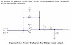
Attached below is the full circuit as recommended by ESS. Anybody recognize the differential output part? Obviously, the parts values are different from the other proposed circuit and have been scaled for optimal SQ in its intended role.
It could be an LM4562. Twisted Pear uses it on their IVY III to sum the balanced signals
Last edited:
Hi freezebox, I would say the madds1 circuit sorta kinda does that, but so far as I am aware nobody has measured it, compared to other outputs for SQ, or done a full and careful analysis of it. Using a 100uf cap to average out the AC component of the inverted output phase (short the audio to ground) and use it to get a very marginally filtered 1/2AVCC isn't very good IMHO compared to a number of other possibilities. As is, a cap would be adversely affecting sound quality, just not in the way everybody seems to be thinking about.
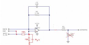
BIG EDIT: Okay, I am just going to say that using the circuit below as is would be expected to give better sound quality than any so-far-seen simple cap removal circuit. If you want easy and good SQ just use it, would be my recommendation.
If you really want to make it even better, and you think getting rid of the cap will help, then you need a more complex circuit. Sorry.
Attachments
Last edited:
freezebox, No, sorry. I was trying to think of something quick like that when I realized ESS only said that circuit works well if both opamp inputs and both DAC outputs are held at AVCC, not 1/2 AVCC.
Not clear how it would work the way I was first thinking of and that you drew. Probably not as well as the circuit ESS recommended otherwise they would have recommended this one.
Thing is, the DAC outputs are a given. They work they way they do and nothing we can do about that. Apparently they like to both be connected to a 1/2 AVCC IV, one DAC output phase at a time, or they like to both go to AVCC sort of together as in the last schematic I posted.
That is what we have to work with. It means there will be an offset unless we want to remove it with some additional circuitry.
Again, it is silly to worry about the sound of one cap, the distortion it gives is probably down around -110dB or -120dB. It is something like that, maybe lower, and if you tried really hard maybe you might just ever so barely be able to hear it, but it is completely negligible unless all the DAC mods and those we haven't done yet are completed. It takes all that to make the DAC really, really clean to the point removing a cap might actually be worthwhile.
Otherwise, as-is now it is a useless distraction, IMHO. People seem to have some kind of fixation on it like it is more important than it is, at least right now.
In the meantime, if the cap is 220uf or more it should be fine. The important thing about electrolytics to remember is that DC voltage on them is not a problem, but to keep distortion really low it can help a lot to keep the AC voltage on the cap very small. Maybe less than 80mV. That means that we want the impedance of the capacitor to be much lower than the impedance of the load that follows it. If you connect the output to a line level preamp or a power amp, the input impedance is probably 10k or maybe a few times greater than that. The electrolytic cap and the load make a voltage divider and we want the AC voltage across the cap to a few millivolts.
So, say the preamp or power amp input is 10k. Say, we are concerned that we want less than 80mV AC on the cap at 10Hz. If the DAC output is 10 volts (peak), then the AC output current will be approximately 1mA. That means there will be 1mA AC current through the cap. If the cap is 220uf, then it's impedance at 10Hz is 72 ohms. With 1mA peak current, the peak AC voltage on the cap will be 72mV. So, we're good!
Last edited:
Moving along, while I am waiting to hear back from an ESS distributor to inquire about non-disclosure and a datasheet, I decided to go ahead a try a couple of other things I have been thinking about. However, I did make multiple changes at once, so can't say for sure how much effect each one has. Sorry.
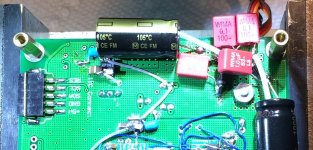
Attached below is yet another photo. After some thought, I decided it might make the most sense to treat the oscillator clock as HF analog, rather than digital. Therefore, it got its own 3.3v low noise regulator. Also added some 1,000uf caps where the power comes into the board. Some film caps were added previously while experimenting with and otherwise working on power supply noise issues.
It turned out that the silent switcher did not like the big 1,000uf capacitive loads and it started causing some odd noises in the DAC output even with the volume all the way down. So, the SS is gone and the DAC and headphone amp are both on the linear power supply.
It sounds very good, but not quite as much of the most subtle details as the reference system which includes a Benchmark DAC-3 and Benchmark ABH2 power amp. The reference system is extremely detailed, probably not wrong to say state-of-the-art detailed. It makes a pretty challenging comparison.
Having made the comparison, the Chinese DAC is still quite good. IMHO, it is definitely a keeper as it is now. It is dynamic, has good well-defined deep bass, detailed and realistic cymbal sounds (one of the hardest things to reproduce accurately in a DAC and amp, it seems), and so forth.
Next steps will be to see if I can get a datasheet here and start testing what can be done to get master mode I2S working.
In parallel with I2S, and as I have time, my notch filter is now working, I need to do some calibration and testing on that. Hopefully, before too long I will be able to post some basic DAC measurements.
Attachments
Last edited:
@tubesguy, My Toslink is on J1, and Coaxial on J2. J3 is the slow transition minimum phase reconstruction filter that sounds so good if upsampling is used. 1.06 board.
Yes, I can see from the ebay listing pics that both versions have the same five headers. All of the listings that I've clicked on recently, however, share the same "documentation" that no doubt accompanied the first versions that were offered for sale, which had six headers, assigned differently.
Future users of the search function for this thread can now find this info. Heck, I'll even add "optical" to the words "Toslink" and "jumper" to help them.
")
May I ask if anyone else is using or planning on using an SRC4392?
How about an LME49600 headphone amp?
I'm still considering the idea of using an SRC4392. Wondering if the Chinese one will be good enough.. (found it on AliExpress too, so easier to buy than on Tababoo (sp)).
I'm building a Dynalo SS (balanced) for my headphone amp.
I have a Chinese SRC4392. Its plenty good enough, I think. Appears to be a genuine SRC4392 chip, and sounds like it too.
To take control of the chip via I2C at some point though will involve tapping into a couple of tiny traces or IC pins on the board. It is quite doable, again I think, although I haven't done this one yet. There are various ways of going about it. I could post some tips and instructions if that's what people need to feel comfortable they can do it.
The only other issue might be the clock quality. I don't know if it will be an issue or not until I get the DAC chip datasheet and start working on master mode I2S. However, the clock could be an issue no matter which one you buy, even a development board from TI. Nobody puts ultra-low jitter clocks on general purpose boards. Such clocks are only for very high-performance systems.
If you did buy a TI development board which I have looked into, they are easy to interface to, bring out all the chip I/O functionality, don't have exceptionally good clocks, are not small, and do not ease learning how to program the chip at all. Cost for that is about $150 vs $60 for the Chinese board. Clock jitter might potentially even be better on the Chinese board than the TI development board, since on the Chinese board the clock is physically located very close to the SRC chip.
As far as using an SRC4392 or not, they make a key difference. It is essential to getting close to DAC-3 or Crane Song 5th generation DAC sound quality. All IMHO, of course. But trust me, it helps a lot even without master mode I2S. You would want to have it if you heard it.
Last edited:
Which one did you buy? I like this one because it has I2S in and out:
Free Shipping! 1pc SRC4392 asynchronous Upconversion with USB coaxial optical I2S Decoder board-in Integrated Circuits from Electronic Components & Supplies on Aliexpress.com | Alibaba Group
It also looks like there should be lots of room to upgrade the Clock chip if needed.
Free Shipping! 1pc SRC4392 asynchronous Upconversion with USB coaxial optical I2S Decoder board-in Integrated Circuits from Electronic Components & Supplies on Aliexpress.com | Alibaba Group
It also looks like there should be lots of room to upgrade the Clock chip if needed.
I like this one because it has I2S in and out:
Yes, that is the one I have. The I2S I/O is all from the A channel. The chip also has a B I2S channel. The B channel pins are not connected on that board, but I think it should probably possible to access them if someone wanted to. Might be worth taking a look at the datasheet and the pinout for the chip. http://www.ti.com/lit/ds/symlink/src4392.pdf
Story: Not long ago I was practising SMD IC removal and replacement on some junk circuit boards. I discovered it is possible to lift IC pins off the board without unsoldering them. In fact, it is a lot easier to avoid involving other pins that way. What I did, under 10x magnification, was take a small jeweller's screwdriver that just fit between the pins and twisted it towards the pin I wanted to lift. With a little gentle wiggling, it came loose, and I got under it with the screwdriver, straightened it out a little and bent it up to where I could have soldered a small wire onto it. Thinking that the pin came up so easily it must have been a fluke, I proceeded to repeat the trick at will on other ICs and boards.
After that, I recalled seeing a youtube video where a guy experimentally repaired an IC with a broken off lead. He dug into the epoxy and exposed only a little of that one pin but enough to solder onto. Feeling emboldened by my earlier success I decided to try it. My jeweller's screwdriver had a new, square, and straight tip on it (something I would recommend for all this) and I was able to use it to dig down through the top edge of an IC and expose the top of only one pin, enough to solder a wire onto using a very small tip.
Everything I did, with sufficient good quality magnification to see clearly, was very easy. At this point, I feel pretty confident about doing such things again. I do not think I ever had the nerve to try it before and wouldn't have thought it could be done reliably.
Why am I saying all the above now? Because it is why I feel very confident I can tap into the I2C bus on the SRC4392 PCB and post pictures of how to do it here. In the meantime, if anybody would like to try practising on a junk PCB maybe it could turn out to be interesting, fun even.
EDIT: Not to worry anyone, I don't think lifting any SRC4392 pins will be necessary, or any other pins on other ICs. It's just one way that could be used to attack the I2C connection problem. Although pin lifting will not be not necessary in this case, tapping into some traces will involve some small work. I will try to make it as easy as possible.
Last edited:
I have successfully tested Toslink, IIS, and DSD of Ver 1.04. The jumper settings and board size of Ver 1.06 on eBay are the same as Ver 1.04. But it's not correct because Ver 1.06 is five jumpers. J02 to J06 probably means J1 to J5 of Ver 1.06.
BTW, I use a cutter knife when I lift a pin of QFT because their blade is thin enough to fit between the pins.
1 PC Utility Knife Large Box Cutter Razor Blade Tool Snap Off Knife Retractable | eBay
BTW, I use a cutter knife when I lift a pin of QFT because their blade is thin enough to fit between the pins.
1 PC Utility Knife Large Box Cutter Razor Blade Tool Snap Off Knife Retractable | eBay
Attachments
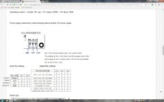
I have successfully tested Toslink, IIS, and DSD of Ver 1.04. The jumper settings and board size of Ver 1.06 on eBay are the same as Ver 1.04. But it's not correct because Ver 1.06 is five jumpers. J02 to J06 probably means J1 to J5 of Ver 1.06.
It is possible that the J1 of board 1.04 sets X or O as default connexion. ? (there seem to be conflicting reports as to which orientation is the select or deselect for J2 etc for Ver 1.04 )
iexample
J1 jumper on and J2 etc are connected when their jumper is present.
J1 jumper off and J2 etc are connected when their jumper is absent.
Will try this when I next have the board out and running.
I found some strange things about the jumper setting of Ver 1.04.
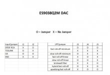
1. IIS is possible both J02=J03=short and J02=J03=open. But J01 must be open. The selection between IIS and DSD depends on the input signal. ES 9038 detects it automatically.
2. Toslink is J02=short and J03=open. J01 is irrelevant. Both short and open is possible. But if you power up the board with J01 short, you can't have the output signal. After powering up with J01 open, you can have the output regardless of J01. But lock LED is off with J01 short. This kind of irregularity sometimes occurs. IMHO, J01 must be open for proper operation. I don't know why you have the output when lock LED is off(J01 short), because I'm not an NDA holder.
I guess Ver1.06 internally makes J01 open.
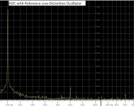
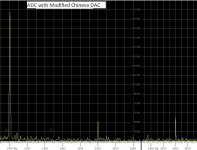
A couple of pictures below. First one is my ADC with one of Victor's low distortion oscillators, so it's essentially ADC distortion only. The second picture is the ADC with my modified Chinese DAC.
EDIT: I should mention that I averaged out some noise.
Obviously, I am going to have to do some more work to get a good measurement, but the implication would seem to be that the DAC distortion is getting reasonably low at this point.
Still no word on my non-disclosure application, so no progress there.
My notch filter at the moment works but is not all that useful for showing pictures due to the use of a Hall network (with its quirks), Maybe another week or so and I will have a twin-T in there and something better for showing images.
Attachments
Last edited:
- Home
- Source & Line
- Digital Line Level
- ES9038Q2M Board