If one wanted to measure AVCC current probably the easiest would be to put a small current sensing resistor in series with the AVCC opamp (or other device) output. It would presumably introduce a little DAC distortion but that could be tolerated for test purposes. A 1-ohm resistor would produce 1mV per mA of current. One could then boost that up with another floating-powered amplifier if the signal was too small for a scope. Maybe a good DVM would be enough to get some idea, don't know. Or one could use a larger value resistor and a scope. The scope could be operated in subtract mode to get a differential reading across the current sense resistor, assuming the scope didn't have a differential vertical amplifier plugin module (which most don't).
Last edited:
I guess LT3042/45 chips are more than fit to provide clean Vref for i/v stage. additional post filtering can be done if necessary. sure, ESS docs available emphasizes clean Vref very much, but again regarding AVCC requirements, it is a little unclear. the regulator has to work in front of a load which will draw some current at some frequency. what here is the most important factor? the usual low impedance over wide frequency range?
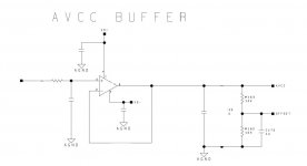
Just to clarify, Vref should be exactly 1/2 of AVCC. So, it is made using two 10k resistors to make a voltage divider with the input of the divider connected to AVCC. A 10uf cap is connected to the output of the voltage divider to filter the output. There is one Vref voltage divider for each channel, since there is one AVCC supply for each channel.
Therefore, there would be no need to use LT3045 to provide Vref unless it was also being used to provide AVCC.
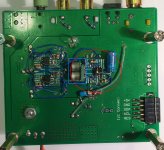
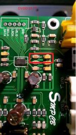
Attached below is a pic of my AVCC supplies (circled in red), and the Vref dividers (inside blue box area).
Attachments
Last edited:
Because my computer crashed and i lost all of files i need some infos before mods.
I have bought V1.07 with display.
What are power supply pin current consumptions and pin confuguration of es9038q2m.
How is with 1,2V pin...regulator...is this voltage regulated inside ic form 3,3V?
No jumper setings were included. For display use i must connected J1 and J2?.. dac plays but lock and dsd leds are not in function. just display shows all parameters?
I have generic apple remote. Did anybody tried remote function ? is it necesary pairing before use?
Thank you Davorin
Last edited:
I only know about the 1.06 board which is the one I have. With all my mods it draws about 130mA on +15v power, and much less maybe 40mA on the -15v power.
Regarding the 1.2v regulator there should be internal regulation but there does need to be bypass caps to ground at that pin. If you measure 1.2 volts there it should be okay.
Maybe somebody with a version 1.07 board can provide more info about the display and settings.
Regarding the 1.2v regulator there should be internal regulation but there does need to be bypass caps to ground at that pin. If you measure 1.2 volts there it should be okay.
Maybe somebody with a version 1.07 board can provide more info about the display and settings.
Looks like there is yet another variant of ES9038Q2M boards starting to appear: ES9038Q2M I2S IIS DSD DOP ????SPDIF????DAC????-???
I am awaiting delivery of an assembled ES9038Q2M DAC with clone Amanero USB, but no power supply. It uses the same VR1.07 board with TFT display. I plan to modify it to accept dual +-15 volts supply using a dual LT1083CP based low noise PS board.Because my computer crashed and i lost all of files i need some infos before mods.
I have bought V1.07 with display.
What are power supply pin current consumptions and pin confuguration of es9038q2m.
How is with 1,2V pin...regulator...is this voltage regulated inside ic form 3,3V?
No jumper setings were included. For display use i must connected J1 and J2?.. dac plays but lock and dsd leds are not in function. just display shows all parameters?
I have generic apple remote. Did anybody tried remote function ? is it necesary pairing before use?
Thank you Davorin
LT1083CP high-power linear hifi regulated DC POWER BOARD KIT two channel output | eBay
I also got an Apple Remote for use with it. I still have to develop plan to change the output to I/V yet.
Make no mistake. This is a low cost, low end approach to Q2M sound. (As compared to Markw4's high end approach.)
Thank you for the encouragement. It is a big IF though.^ Really though, if you can get any of the I/V circuits described in this thread to work for you, it will be a high end piece.
") For a total outlay of less than $160, I am hoping to get reasonable SQ without the I/V output, which can tile me over for awhile.
For a total outlay of less than $160, I am hoping to get reasonable SQ without the I/V output, which can tile me over for awhile.This seems to be a popular ES9038Q2M board, widely available and priced reasonably. I am surprised that no one developed a I/V daughter board to replace the NE5532 yet.
Last edited:
I did some measurements on original board using 12v Accu to eliminate transformer influence of unshielded board... measured filters, response, pulse response...
Specs are ok for that board... most bothers me 1.2v line that has big noise that polute other 2 pins for 3,3v in nearby trought GND line. I think GND should be splitted at least in some distance to eliminate direct oscilation on that position.
I will be using transformer output so opamps don*t interest me. maybe later tube out if result will be promising.
Btw... best pulse response has linear phase rollof but worst thd at 15-20khz region and around -6db at 20khz in 44.1khz input
second best are apodising and brickwall... worst are both minimum phase with huuuuge preringing...
Digital volume is doing quite qood job i think something was done in that way because at es9018 volume has bigger influence in SQ.
Next step is installing regulators at each power supply line... and cutting and splitting some gnd routes...
Well I thought about it and looked over the recommendations from ESS, What I had initially missed was that the single op amp IV solution actually runs off a single 12V supply and can use the same rail that powers the op amp for AVCC. There is no need for a voltage divider and this can bring some benefits as well I think because there is less error in getting an accurate bias voltage.
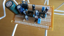
So for the sake of curiosity, I was halfway through laying out the opamp AVCC and the three op amp IV circcuit and the voltage divider. then I was bitten to step back and see just how well can someone expect to modify this DAC in a relatively simple fashion without making custom boards.
So on a piece of 2x3" perfboard, I was able to put in 3 terminal power supply that will produce the single 12V required to power two dual op amps. One dual will provide 2xAVCC fed from a single filter from a feed from the AMS1117. I will simply tap off some voltage from the large soldered tab on the AMS1117. The other dual op amp will utilize the IV circuit as recommended by ESS for a budget IV. None of the parts I used is exotic or high performance intentionally. I want to see how good or bad it gets with simplicity. I should be able to swap op amps ranging from TL072. AD712 LM833, OPA2134 , NE5532 and then LME49720.
On the DAC, the 12V will power only one leg where normally the +15V will be. This 15V is regulated down to 5 V and then to 3.3 etc. The analog portion of the DAC will be completely external.
Why do this? Because I think I might have meandered too much in trying to get this dac to work well. I am now of the thought that one should first focus on the AVCC first ( use the OP AMP regulator, then put in a current IV..the one ESS recommends for simplicity is as simple as it gets, I suspect that after this, the only other mod that needs to be considered is then a crystal upgrade and then.....maybe the resampler. I just want to know. In reality what I am doing could have been on the DAC in the first place and can't figure out why they didn't?
Oh, I am still proceeding on using a 3042 simply to feed the 3.3V other than AVCC and use that as the basis for the reference voltage. With the divider and 3 opamp IV fed by low noise fast regulators as well. It will be an interesting summer.
Markw4 might want to add some comments.
Attachments
Last edited:
So I will bring two voltage lines from the board to the AVCC
I will cut the two traces that lead to AVCC
I will remove the resistors from the DAC lines on the board and use the pads as a feed source.
I will then bring out the four DAC lines from the DAC board to my external IV.
I will feed the DAC with the 12V generated by the 3term regulator on the external board.
I will remove the op amp from the DAC and then that should do it.
@andora76, The minimum phase filters don't pre-ring. If it looks like they appear to be doing that it could be that the wrong filters are being selected by the jumpers.
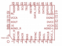
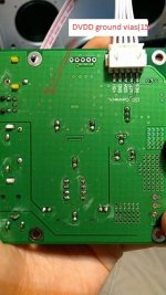
The 1.2v pin should have two bypass caps to ground very close to the pin. It is the pin labeled DVDD in the diagram below. Is that where noise is being seen, and if so what does it look like?
The 1.2v pin should have two bypass caps to ground very close to the pin. It is the pin labeled DVDD in the diagram below. Is that where noise is being seen, and if so what does it look like?
Attachments
Last edited:
Great news! The super cheap apple remote works with my 1.07 board! (my board wasn't supposed to have a remote). The apple clone remote cost 3 usd!. It has very poor fit'n finish so I might buy one in aluminium now that I know it works I have the version with a stock rotary encoder pot connected to the screen, and now the remote lets me control all the functions.
I have the version with a stock rotary encoder pot connected to the screen, and now the remote lets me control all the functions.I am still proceeding on using a 3042 simply to feed the 3.3V other than AVCC and use that as the basis for the reference voltage.
I don't understand what you mean about using a 3042 to make the reference voltage for the IV stages. It makes no sense to me unless you are using the same 3042 to power AVCC.
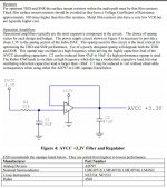
Please see the diagrams below. The point marked "offset" is another name for "reference voltage." That is the correct way to make the reference voltage.
Attachments
So I will bring two voltage lines from the board to the AVCC
I will cut the two traces that lead to AVCC
I will remove the resistors from the DAC lines on the board and use the pads as a feed source.
I will then bring out the four DAC lines from the DAC board to my external IV.
I will feed the DAC with the 12V generated by the 3term regulator on the external board.
I will remove the op amp from the DAC and then that should do it.
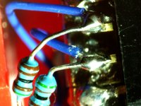
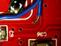
Don't forget a nice low impedance ground connection between the boards that is effective at HF and ideally at RF. Personally, I think there is some advantage to making the connections from the solder side (ground plane side) of the DAC board. Easy to do with any kind of a very small drill or burr. Only needs a big enough diameter to pass a very thin wire-wrap type wire through. It is also quite safe to make holes through the DAC board since it is only 2-layer (2-sided). There is no chance of hitting a hidden layer conductor inside.
BTW, Digikey has some little 25-foot spools of 32AWG stranded wire for cheap compared to their normal wire prices. Around $8/spool. Between that and some 28-30 solid wire-wrap wire it is possible to do just about any small unshielded wiring one might want to do.
In addition to the wire, a small solder iron tip and an iron with a temperature control, a sharp point Exacto knife, and some .4mm diameter solder (all available from Amazon or wherever, Amazon also has wire-wrap wire) is all that is needed to do any of the tiny work I have done. Mostly it just takes some practice on scrap circuit boards. Chem-wick type solder wick is helpful too. 100% isopropyl alcohol and a little brush cleans off most flux. All available at Amazon.
Some mods I did to the little SRC4392 board to get access to the I2C bus were done using the above listed tools and supplies. It was quite easy with the right stuff on hand. See some pics below to get an idea.
Attachments
Last edited:
I don't understand what you mean about using a 3042 to make the reference voltage for the IV stages. It makes no sense to me unless you are using the same 3042 to power AVCC.
Please see the diagrams below. The point marked "offset" is another name for "reference voltage." That is the correct way to make the reference voltage.
I was thinking of using the low noise 3.3V from the 3042 and filter that to feed the op amp input which will power AVCC.
The initial board will be by the book according to ESS document where the reference voltage is AVCC itself on the + input of the op amp for the IV stage
Last edited:
I was thinking of using the low noise 3.3V from the 3042 and filter that to feed the op amp input which will power AVCC.
Okay, I do get that. Thanks for clarifying for me.
- Home
- Source & Line
- Digital Line Level
- ES9038Q2M Board