Hello,
I'm designing a audio digital board for a power amp.
Purpose of these board is to have 3 digital input: 1 USB UAC, 1 SPDIF, 1 Bluetooth and one analog input.
My design is based upon a stm32f446 (open uac2 project ), a Microchip BM83 module for BT and a ES9038q2m for the dac.
ES9038 looks good choice for me as he directly have a spdif input (fews days ago I think about a SRC4392 and a AK4490 combo, ES9038 look cheaper and simpler).
Then STM32 feed dac with one I2s, there is another I2S from BM83 module and a simple mux will do the job of routing I2S signal to the dac.
For clocking section I think using directly the stm32 MCO output (openUAC2 project give a MCO clock output wich is 22.5792 or 24.576 depends of 41/48k fs family) to give ES9038q2m a clock.
My plan here is to have a 'perfect' Fs when USB is selected (STM32 give 22.5792 or 24.576) and when other input selected (BM83 ou SPDIF) stm32 is set to 24.576: so when bm83/spdif is 48k family I have a perfect Fs, when 44.1k family the dpll inside ES9038q2m give me a not too bad 44100.002288 Fs.
For I/V conversion I think about a classic 2 order LPF using OPA1612:
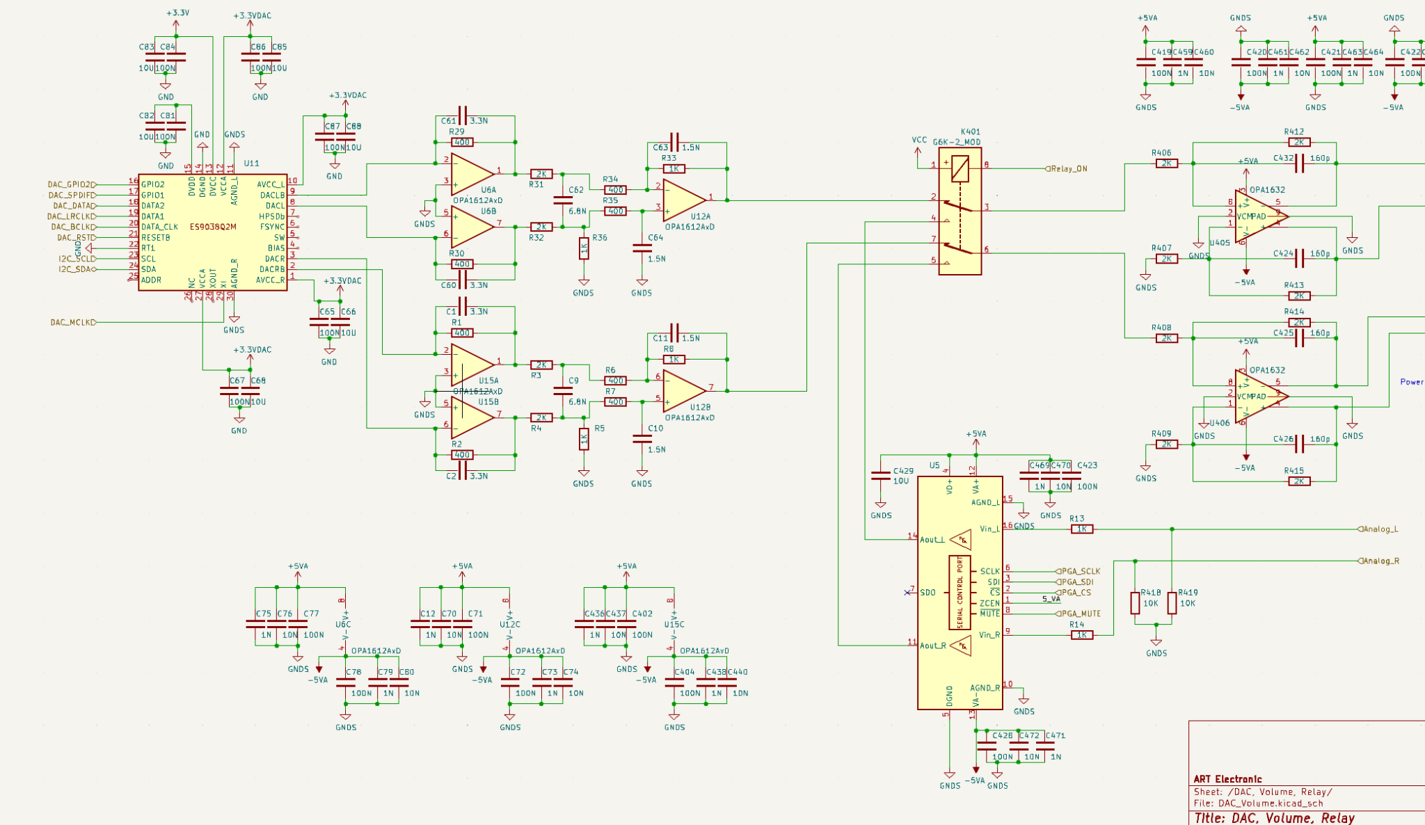
Are there any big mistake I did on these implementation ?
If you have feedback I will be interested
have a good day!
I'm designing a audio digital board for a power amp.
Purpose of these board is to have 3 digital input: 1 USB UAC, 1 SPDIF, 1 Bluetooth and one analog input.
My design is based upon a stm32f446 (open uac2 project ), a Microchip BM83 module for BT and a ES9038q2m for the dac.
ES9038 looks good choice for me as he directly have a spdif input (fews days ago I think about a SRC4392 and a AK4490 combo, ES9038 look cheaper and simpler).
Then STM32 feed dac with one I2s, there is another I2S from BM83 module and a simple mux will do the job of routing I2S signal to the dac.
For clocking section I think using directly the stm32 MCO output (openUAC2 project give a MCO clock output wich is 22.5792 or 24.576 depends of 41/48k fs family) to give ES9038q2m a clock.
My plan here is to have a 'perfect' Fs when USB is selected (STM32 give 22.5792 or 24.576) and when other input selected (BM83 ou SPDIF) stm32 is set to 24.576: so when bm83/spdif is 48k family I have a perfect Fs, when 44.1k family the dpll inside ES9038q2m give me a not too bad 44100.002288 Fs.
For I/V conversion I think about a classic 2 order LPF using OPA1612:
Are there any big mistake I did on these implementation ?
If you have feedback I will be interested
have a good day!
Looks like there are some things you might want to consider. First is that a good output stage is not all that a dac needs. It also needs a good time reference and a good voltage reference. For ESS dacs the voltage reference is called AVCC, whereas for some other dacs it may be called something like Vref. In particular, ESS dacs should have two separate voltage regulators right next to the dac chip, since there is one voltage reference needed for each of the stereo channels. If you tie AVCC to the other dac power pins, its going to sound bad. On the issue of the time reference, you need a pretty good crystal clock right next to the dac chip. I use a regulator for it too since clocks are basically analog circuits, not digital.Are there any big mistake I did on these implementation ?
In general, the quality of a dac is not so much a function of the dac chip as it is a function of the quality of the circuitry around the dac chip, and of layout. That said, the newer ESS ES9039Q2M has been claimed to have better sound than the older ES9038Q2M. However, to get that better sound you still need to take care of AVCC and the clock or clocks (you can use two clocks if you want to avoid the internal ASRC in ESS dac chips, at least for cases where it shouldn't be needed, which is to say for well designed USB.
Other things could be said about the output stage design if you want differential outputs. Maybe better to avoid going SE in the first place,
Also, the output stage topology recommend for the newer ES9039Q2M may turn out to sound better than what they were recommending back when ES9038Q2M came out. Don't know. Haven't tried it.
Last edited:
There is some shematics we can found with small ferite bead/resistor to gently decouple power rails:
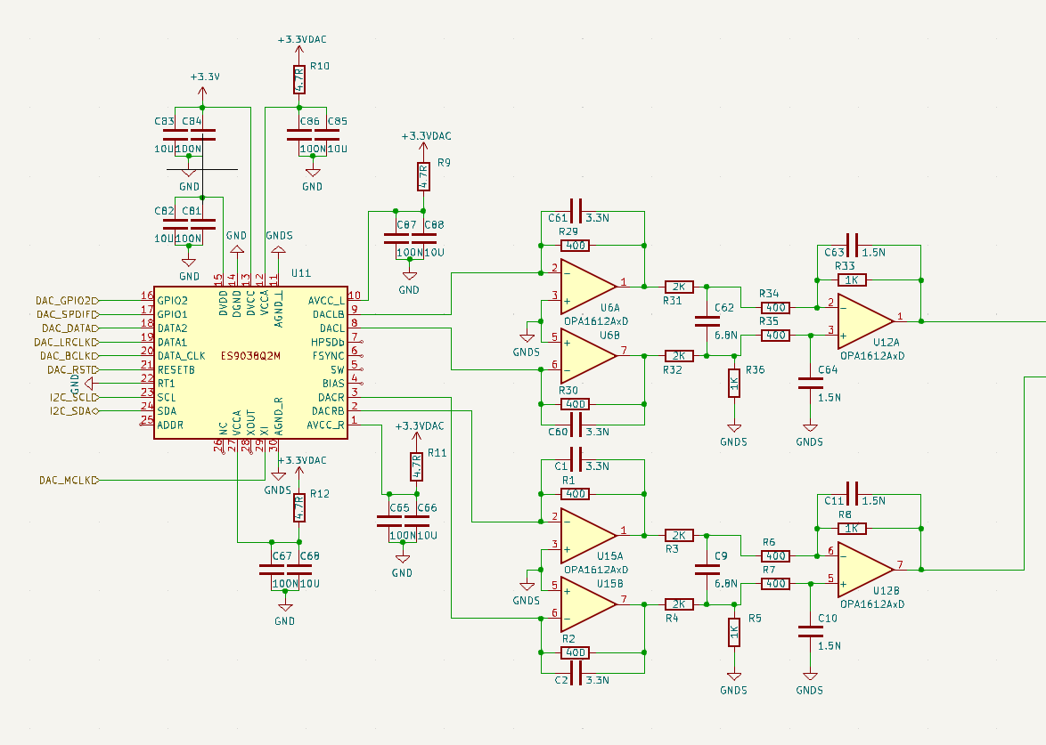
I also can use electrochemical caps on AVCC_R/L power inputs to have more decoupling between them and other VCCA inputs.
I'm loking specifically on clock settings and possibilities.
I really don't know if avoiding ASRC is a good thing or not, my use case is: USB UAC asynchrone with a local clock or Bluetooth from a BM83 module or SPDIF input. I imagine ASRC operation of the dac is a good thing for Bluetooth or SPDIF but maybe not necessary for USB UAC audio as it already have a good local reference for clock.
This IC can be used with a local 100Mhz reference clock to do ASRC with following performance in terms of final Fs:
47999,993 Hz for 48k
44100,0098Hz for 41k
using following formula given in datasheet:
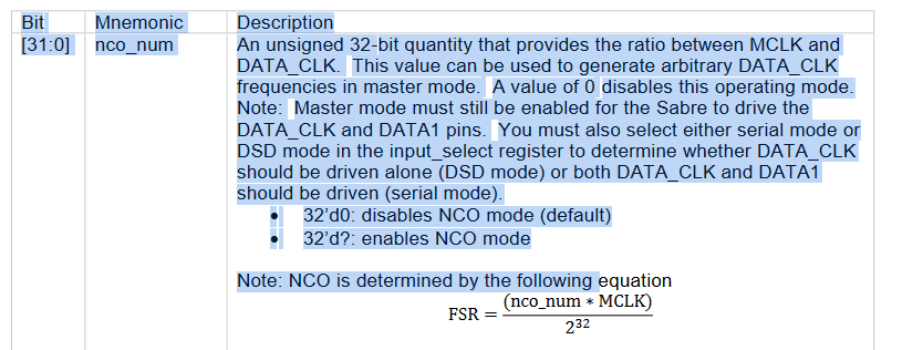
Because my design hown a good local clock which can generate audio frequency 22.5792 or 24.576M, thanks to the open UAC project, I imagine using this clock to feed the dac when playing from USB UAC I2S to get exact Fs instead of 100Mhz reference. I don't know if using ASRC in this case is a good thing ?
But an old version of ESS datasheet made me afraid about using 22.5/24M clock on Xi pin:


With 22.5/24M the max Fs will be limited to 96k in PCM input and 48k in SPDIF mode. I want achieve at least 192ks Fs.
So I have to double and feed dac with 45.1584Mhz/49,152Mhz at least if I want go to 192ks. I don't know if the master clock output of my stm32 can achieve such 'high' frequency (for 24M frequency I know this is ok).
To resume I'm beginner in digital audio, it's a hobby for me and a fun way to learn about frequency domain adaptation process (I'm electronics professional and play with hifi amp in my homelab for fun)
I understand that ASRC operation inside DAC is not necessary when feeding it with correct audio clock (ie 45.1xx or 49.xx accordingly to Fs rate of I2S bus). ASRC can lower jitter with other I2S source like Bluetooth, in that case is a good thing using ASRC to reduce jitter because the oscillator of the BT module can be high (don't know).
ASRC can lower jitter with SPDIF input also.
So don't know is it's best to use 100Mhz like in es9038 datasheet or if there is a good opportunity to use my local oscillator from the stm32.
For the I/V stage I prefer use the classic topology (wich I already sucessfully implemented with a TI PCM1792 dac).
You right it looks silly to goes SE just before going again diff, but in my design it's the simplest way (cost one opamp instead of another relay).
It would be helpfull ES give layout example, especially regarding digital ground domain and analog ground domain, i don't know where to joins them (just below the dac ?)
I also can use electrochemical caps on AVCC_R/L power inputs to have more decoupling between them and other VCCA inputs.
I'm loking specifically on clock settings and possibilities.
I really don't know if avoiding ASRC is a good thing or not, my use case is: USB UAC asynchrone with a local clock or Bluetooth from a BM83 module or SPDIF input. I imagine ASRC operation of the dac is a good thing for Bluetooth or SPDIF but maybe not necessary for USB UAC audio as it already have a good local reference for clock.
This IC can be used with a local 100Mhz reference clock to do ASRC with following performance in terms of final Fs:
47999,993 Hz for 48k
44100,0098Hz for 41k
using following formula given in datasheet:
Because my design hown a good local clock which can generate audio frequency 22.5792 or 24.576M, thanks to the open UAC project, I imagine using this clock to feed the dac when playing from USB UAC I2S to get exact Fs instead of 100Mhz reference. I don't know if using ASRC in this case is a good thing ?
But an old version of ESS datasheet made me afraid about using 22.5/24M clock on Xi pin:
With 22.5/24M the max Fs will be limited to 96k in PCM input and 48k in SPDIF mode. I want achieve at least 192ks Fs.
So I have to double and feed dac with 45.1584Mhz/49,152Mhz at least if I want go to 192ks. I don't know if the master clock output of my stm32 can achieve such 'high' frequency (for 24M frequency I know this is ok).
To resume I'm beginner in digital audio, it's a hobby for me and a fun way to learn about frequency domain adaptation process (I'm electronics professional and play with hifi amp in my homelab for fun)
I understand that ASRC operation inside DAC is not necessary when feeding it with correct audio clock (ie 45.1xx or 49.xx accordingly to Fs rate of I2S bus). ASRC can lower jitter with other I2S source like Bluetooth, in that case is a good thing using ASRC to reduce jitter because the oscillator of the BT module can be high (don't know).
ASRC can lower jitter with SPDIF input also.
So don't know is it's best to use 100Mhz like in es9038 datasheet or if there is a good opportunity to use my local oscillator from the stm32.
For the I/V stage I prefer use the classic topology (wich I already sucessfully implemented with a TI PCM1792 dac).
You right it looks silly to goes SE just before going again diff, but in my design it's the simplest way (cost one opamp instead of another relay).
It would be helpfull ES give layout example, especially regarding digital ground domain and analog ground domain, i don't know where to joins them (just below the dac ?)
We have built dacs like this both ways. Also there is an old app note from ESS. I will see if I can attach it. It says to put the AVCC regulator very close to the AVCC pins, and on the same ground plane. IME, even then there is more to know about getting it to sound good than they wrote about.There is some shematics we can found with small ferite bead/resistor to gently decouple power rails...
Regarding clock frequency, distortion and noise are somewhat clock frequency dependent. Lower clock frequencies are probably better, but they limit the maximum music sample rate it can handle. NDK SDA series clocks are decent for this application. Synchronous operation can use lower clock frequencies for a given sample rate, but the circuitry requires two clocks and external clocking for the USB interface (or you could use the USB board clocks, but not as good).
Attachments
Last edited:
If you want to build this thing simply and at low cost, there are options though... Victor's solutions for the Chinese dac boards of this thread is sort of an intermediate way of getting better measurements, while still keeping the circuitry pretty simple.
Regarding the USB boards, the best results are probably with I2SoverUSB (fully isolated version) using two isolated +5v power supplies. It has decent NDK SDA clocks, galvanic isolation, and can output 45/49MHz clock frequencies you need for 24/292 playback support. http://www.jlsounds.com/i2soverusbFIO.html
Analog and digital grounds have to meet at the dac, as you say. That's if you are going to use two separate ground planes, but you don't have to. It might be better just to layout the board mindful of where ground currents will flow. The problem with split ground planes (analog and digital) is that they can make good transmitting antennas (called a "slot" antenna). You can use two board layers as separate ground planes, but there will still be some coupling between them. In any case use at least a 4-layer board.
Regarding non-USB digital inputs to the dac, you may need the ASRC for that. So you may want to think about what sample rates you need to support in that usage case.
Last edited:
Tell you what, I will put the ES9038Q2M eval board design package in my dropbox at: https://www.dropbox.com/scl/fo/b25l11lijp8lb07hpw6at/h?rlkey=ma8zxn69cu9mgkr9oc0k546z9&dl=0
The PCB design program they used is DipTrace. You can download a trial version if you want.
BTW, not everyone agrees the ESS design is exemplary. Its just one option.
The PCB design program they used is DipTrace. You can download a trial version if you want.
BTW, not everyone agrees the ESS design is exemplary. Its just one option.
you may need the ASRC for that
Why? ASRC is already inside ES9038.
@__BriKs__
You also may be interested to know that some us have moved past using dac chips. IMHO and IME we can get better sound using discrete resistor dacs. There are some open source options for doing that, as well as pre-designed boards that be integrated into an overall design by a good diy'er. Some of these discrete resistor dacs are getting into in the big league of dac sound quality. Maybe pretty close to Bruno Putzeys' Mola dacs in that regard.
You also may be interested to know that some us have moved past using dac chips. IMHO and IME we can get better sound using discrete resistor dacs. There are some open source options for doing that, as well as pre-designed boards that be integrated into an overall design by a good diy'er. Some of these discrete resistor dacs are getting into in the big league of dac sound quality. Maybe pretty close to Bruno Putzeys' Mola dacs in that regard.
ES9038Q2M datasheet states that in PCM mode minimum MCK is 128FS (sync) or 192FS (async). So with 22M/24M clocks you can have 192k FS in sync mode. Async mode requires separate clock so in that mode your stm32 board clocks are not used.With 22.5/24M the max Fs will be limited to 96k in PCM input and 48k in SPDIF mode. I want achieve at least 192ks Fs.
The I/V converters are not quite classic. Normally the + inputs of the op-amps would be connected to a reference voltage, typically at half the AVCC_L and AVCC_R. Does it work with the + inputs grounded? It will force the outputs of the ES9038Q2M to GND level.For I/V conversion I think about a classic 2 order LPF using OPA1612:
Are there any big mistake I did on these implementation ?
If you have feedback I will be interested
The resistors R36 and R5 should be connected in parallel with C64 and C10 respectively. Otherwise the common mode rejection of the differential amplifier/filter will be very poor.
Hi, many thanks for all yr feedback! This help me understand how to manage a dac.
Attached schematics of my design, this way is more easy to explain what I want to do.
The USB audio is on the same board, managed with STM32 wich acts as a general purpose controler and a USB UAC2 streamer. So I use audio clock generated by STM32, register configurable for 44.1k/48k family and normally can goes up to 98.304M/90.3168Mhz, will try when PCB where ready. The clock is buffered by a MUX (I have to find if TMUX1574 act as a buffer or not, if not going on SN74 circuitry).
With this scheme when USB input DAC will run without ASRC with proper audio clock automatically managed by STM32, if SPDIF or BT input the clock is set to 48k family and ASRC is ON.
@Markw4 thanks for give me AN from ES, indeed will use a 4l pcb, also today my schematic show different gnd domain, I think will keep just one with proper current path as you say this is the way to go my last work design use only one plane and achieve very good SNR. I will take a look on Victor's solution, hard to find on the 398 thread sheets . Also will take a look on NDK SDA serie, but seems not easy availlability (mouser, digikey...). For now I will stay on a IC design for DAC, but design with discrete r2r looks beuatifull indeed!
@altor : BM83 looks easy to use with sample config code on github, as my favorite programing langage is definitly iron solder nor embeded C, I choose BM83 for this reason and also mouser availlability. If you know other module I'm interested in.
@bohrok2610 Yes when SPDIF/BT is selected as input I will clock the DAC with a fixed frequency derived from 48k family.
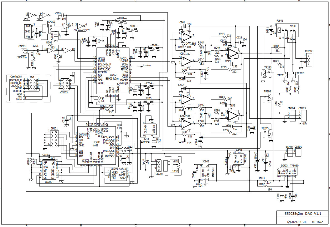
@JensH: You focus on very interesting thing, today I simply reuse schematic I found on this forum:
And also find a ltspice of AFE of ES9038 on internet:
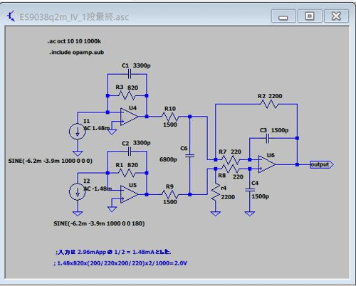
For me there is only R7 and R8 (ltspice shematic below) who differs from what you says about common mode rejection, R7 and R8 only change the behaviour of the last diff to se amplifier, adding a pole to make the frequency answer more flat. But will be interested in to understand your feedback about common mode rejection. For the other thing, the gnd connected to n inverting input indeed you totally right, this will push DAC out near GND, will made a HW conf here with mounted/not mounted resistor, thanks to you!
Attached schematics of my design, this way is more easy to explain what I want to do.
The USB audio is on the same board, managed with STM32 wich acts as a general purpose controler and a USB UAC2 streamer. So I use audio clock generated by STM32, register configurable for 44.1k/48k family and normally can goes up to 98.304M/90.3168Mhz, will try when PCB where ready. The clock is buffered by a MUX (I have to find if TMUX1574 act as a buffer or not, if not going on SN74 circuitry).
With this scheme when USB input DAC will run without ASRC with proper audio clock automatically managed by STM32, if SPDIF or BT input the clock is set to 48k family and ASRC is ON.
@Markw4 thanks for give me AN from ES, indeed will use a 4l pcb, also today my schematic show different gnd domain, I think will keep just one with proper current path as you say this is the way to go my last work design use only one plane and achieve very good SNR. I will take a look on Victor's solution, hard to find on the 398 thread sheets
@altor : BM83 looks easy to use with sample config code on github, as my favorite programing langage is definitly iron solder nor embeded C, I choose BM83 for this reason and also mouser availlability. If you know other module I'm interested in.
@bohrok2610 Yes when SPDIF/BT is selected as input I will clock the DAC with a fixed frequency derived from 48k family.
@JensH: You focus on very interesting thing, today I simply reuse schematic I found on this forum:
And also find a ltspice of AFE of ES9038 on internet:
For me there is only R7 and R8 (ltspice shematic below) who differs from what you says about common mode rejection, R7 and R8 only change the behaviour of the last diff to se amplifier, adding a pole to make the frequency answer more flat. But will be interested in to understand your feedback about common mode rejection. For the other thing, the gnd connected to n inverting input indeed you totally right, this will push DAC out near GND, will made a HW conf here with mounted/not mounted resistor, thanks to you!
Attachments
TLV755 has far too much noise for AVCC supply. Use it only for VCCA & DVCC and a lower noise regulator for AVCC.
Using MCK generated by STM32F4 will likely have quite a lot of jitter no matter what oscillator you use. It is much better to have separate low jitter clocks for audio MCK and use those clocks for I2S generation via PC9. But that would need changes to the FW you are planning to use. Easier and lower jitter solution for you would be to use ASRC also for USB.
Using MCK generated by STM32F4 will likely have quite a lot of jitter no matter what oscillator you use. It is much better to have separate low jitter clocks for audio MCK and use those clocks for I2S generation via PC9. But that would need changes to the FW you are planning to use. Easier and lower jitter solution for you would be to use ASRC also for USB.
@__BriKs__
The schematic for the differential amplifier/filter you show in post #7,958 is not the same as the one you have in post #7,948!
In the schematic in post #7,948 you need to move R8 and R33. And yes, this is better than moving R36 and R5. The cut-off will be sharper when moving R8 and R33, although with a bit of peaking.
- Home
- Source & Line
- Digital Line Level
- ES9038Q2M Board