They use TPS7A49 + OPA1612 OPAMP Buffer to power up vref_r and vref_l.
What is strange as far as i saw they use only positive power supply for the opamps.
what sorcery is this?
I strongly suspect that there are positive and negative regs on the board for the output opamps VCC/VEE. The VCCA opamp is better off with its VEE pin connected to ground anyways because it only has to deliver positive output voltage.
What i do not understand;
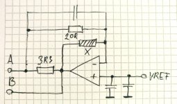
The function of use lots of STO-23+ 10k resistors components.
What is 16 pin qfn ic just before for each outputs (3 pcs marking:3710 / 2007U)
Why they use resistor and capacitors in the feedback for vref buffer opamp
The 16 pin qfn is most likely the mute circuitry, but nothing to be found on this chip, at least MY search foo was not good enough
")
regarding the feedback circuitry around the AVCC opamp - I tried to reverse engineer this. Don't know if I got it correctly:
Part with designator "X" could be a small ferrite bead (it's grey in the foto) or a cap (unusual color for a cap, all the other ones are yellow/brownish)
Also I don't know what is supposed to be the output of the circuit - A or B. Can't see in the picture as the trace to the DAC's AVCC pins dips below the top layer and I cannot tell wether it's from A or B. I suspect it's A...
Maybe someone with more insight to MFB technology could shed some light on this?
Attachments
Last edited:
I strongly suspect that there are positive and negative regs on the board for the output opamps VCC/VEE. The VCCA opamp is better off with its VEE pin connected to ground anyways because it only has to deliver positive output voltage.
The 16 pin qfn is most likely the mute circuitry, but nothing to be found on this chip, at least MY search foo was not good enough
regarding the feedback circuitry around the AVCC opamp - I tried to reverse engineer this. Don't know if I got it correctly:
Part with designator "X" could be a small ferrite bead (it's grey in the foto) or a cap (unusual color for a cap, all the other ones are yellow/brownish)
Also I don't know what is supposed to be the output of the circuit - A or B. Can't see in the picture as the trace to the DAC's AVCC pins dips below the top layer and I cannot tell wether it's from A or B. I suspect it's A...
Maybe someone with more insight to MFB technology could shed some light on this?
I tried lots of simulation but not able to get better noise rejection performance.
I just fired up LTspice as well. What values did you use for the sim. Did you use a cap for "X"?
I tried lots of values between 1n to 100u. And tryed lots of different ferrite bad in ltspice standard library. Nothing changed in a good way in the means of noise but it could be for stablity for sure.
Topping chose +-11v rails for D90. I wondered why since opamps often sound better with higher rail voltages. Tried every voltage in one volt increments from 10v to 15v. Agree with Topping on their choice. +-11v sounded best to me. Haven't done the same experiment with an ESS dac though. I would suggest to try it yourself and see what you think. Its easy enough to do if the regulators have adjustment pots with enough range.
Also IMHO a lot of stuff affecting SQ can be determined with experiments and listening tests (mostly for analog circuitry and power supplies; not so much for digital). Good to be careful deciding what is analog and what is digital. For example clock oscillators are analog. We may hear from some people who disagree on this topic though.
Also IMHO a lot of stuff affecting SQ can be determined with experiments and listening tests (mostly for analog circuitry and power supplies; not so much for digital). Good to be careful deciding what is analog and what is digital. For example clock oscillators are analog. We may hear from some people who disagree on this topic though.
Last edited:
Hello @Markw4
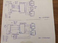
I would use two ES9038Q2M in mono mode for playing PCM and DSD up to highest rates with I2SoverUSBv.III.
I´ve attached a sketch showing the clock distribution:
- first one with external buffered 100MHz clock to the two DAC XI inputs
- second one with buffered MCLK from USB receiver to the two DAC XI inputs
- third solution (not sketched) would be external MCLK also for USB receiver
What for solution is proven and gives good results?
JP
Attachments
Hi JPS64,
I can tell you what I would recommend for the digital front end and clocking. My choice would be to use two clocks (both running at all times, the output frequency selected with a small signal relay with gold contacts). Buffer the relay output with something like NB3L553-D or maybe PL133-27. Might try 805 SMD film caps for clock and buffer bypass. Route clocks from the buffers to the dac chips and to the I2SoverUSB card external clock input. Use the isolated signal from I2SoverUSB to operate the clock frequency selection relay. You can relcock I2S coming from I2SoverUSB, but it has already reclocked there once in a CPLD. You could probably get I2S jitter a little lower with one more reclock near the dac chips, as you show. Sometimes it helps to use larger than predicted series termination resistors at the output of the relclock chip, say, maybe 100-ohms (instead of, say, maybe a more typical 33-ohms). Its one of those things you have to try and see if it helps in your design situation.
It means the dac chips would need to be controlled by some MCU to set the registers for synchronous operation. IME, ESS dacs tend to sound better that way, at least they do for me.
If implemented more or less as above, then the only remaining problems to work out would be AVCC regulation and output stage design.
The above assumes everything is well laid out on a 4-layer PCB with a ground plane. Good to have maybe a +5v power plane or large fill area on one layer. Then local regulators can drop it down to +3.3v as needed near loads such as clocks, buffers, and various dac chip power rails.
Last edited:
Something like that, but I personally would not use clock select pins on the clocks since IME its not the same as leaving them fully running at all times. Also, I'm not a fan of using ferrite beads unless they are proven necessary to solve a problem in a particular design. My unproven suspicion is that they could produce some hysteresis distortion/noise that could cause its own problems. However one could leave pads for ferrite beads and put a zero ohm resistor on the pads if a ferrite bead is not found to be needed during testing.
There are various small signal relays with gold contacts. One of the smaller types is: https://omronfs.omron.com/en_US/ecb/products/pdf/en-g6k.pdf
or maybe even better:
https://omronfs.omron.com/en_US/ecb/products/pdf/en-g6k_2f_rf.pdf
Regarding a 'driver' for ES9038Q2M, what do mean by that? Software to control the registers?
or maybe even better:
https://omronfs.omron.com/en_US/ecb/products/pdf/en-g6k_2f_rf.pdf
Regarding a 'driver' for ES9038Q2M, what do mean by that? Software to control the registers?
People have done it to some extent with command line scripts using RPi. For some other linux platform one might need some kind of a hardware interface, say, maybe USB to I2C. Figuring out how to program the registers isn't too hard. Besides, now that ESS has released ES9038Q2M datasheet we are free to talk about register programming here.
Please let us know how to set up for such test so that we can try and see for ourselves.Also IMHO a lot of stuff affecting SQ can be determined with experiments and listening tests (mostly for analog circuitry and power supplies; not so much for digital).
- Home
- Source & Line
- Digital Line Level
- ES9038Q2M Board