My plan: Dual mono ES9039Q2M. Power supply (not shown) will use 3x discrete shunt 3.3V. My PSU was not tested yet. But I have made +-15VDC and 5VDC discrete shunt regulator. Basic shunt regulator from Walt Jung (he used op-amp).
Be aware that THD performance will be in the range of -70 dB. This link shows typical ES9038Q2M measured performance without a proper I/V converter output stage: Measurements Of Generic ES9038Q2M DAC Board | Audio Science Review (ASR) Forum
If you instead use the I/V output stage in post #6944 you can get performance like what I posted in #6981.
So the power supplies are important but if you don't use the correct output stage with this DAC the results will be very poor.
I would agree that the component values in #6944 might be better, but it should depend on which opamps you use, layout, etc. Kozard did some early phase testing with opamps he had on hand, and without a more ideal output stage board. Speaking for myself only, too soon to draw final conclusions.
Last edited:
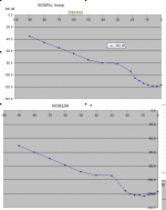
Sure. I am just trying to communicate (with the graphs) the degradation to around -70 dB range (instead of -120 dB range) due to the lack of a proper I/V output stage. I think the approximate 50 dB difference is night and day. (And can not be ignored.) One sounds very bad (worse than a cheap CD player in 1987) while the other is much much better.
I don't want someone to design and build a board with all sorts of cost just to end up with -70 dB performance because the importance of a proper I/V output stage was not understood.
The ES9038Q2M is not a CS4398 or AK4396. If someone has experience with CS4398 or AK4396 they might think that a voltage mode output isn't terrible. But they would misunderstand that the ES9038Q2M doesn't work well (at all) without the proper I/V stage. I think some misunderstand and think that the board designer makes the choice between voltage mode and I/V stage. Instead perhaps they should consider that the ES9038Q2M internal design is intended for I/V output and will be severely degraded otherwise. Other DAC chips are designed for use with voltage mode output.
Hi Bimo,
There is a pretty good paper that ESS published before they decided to go NDA (more recently, they decided to lift most of the NDA secrecy). Its available on their website: http://www.esstech.com/index.php/download_file/view/69/267/ ...Highly recommend it for careful study to start with. Not just the schematics either, all of the text is important to keep in mind.
Thank you for the document. The guide is normal in engineering, not really new to me, but I will read them several time with careful. May be I miss something.
Actually, I draw schematic for ES9038PRO, too. But I think I will try ES9038Q2M first. I don't worry about pcb layout. The analog filter and power supply are my concern.
Some of the voltage regulators don't need to be shunt types. It just doesn't help for some things. Its more important the enough local regulators are used close to the dac chip and on the dac board ground plane. PCB needs to be at least 4-layers. VCCA, DVCC, and the clock all benefit from their own dedicated regulators. AVCC_L and AVCC_R are the most critical power supplies. The ESS document makes clear they need to be close to dac chip and wide traces used so as to keep impedance low. VCCA is analog power for clock related RF frequencies. DVCC is for digital processing. Some of the loads work fine with LDO regulators. Not AVCC though. Shunt regulators for it might sound great, but they need to be close to the dac or large, expensive rolled foil and film decoupling caps may be need to correct the sound deficit. There are more layout worries that will affect performance. The analog filter is processing clock noise and frequency-shaped random noise all mixed in with the audio. A significant issue is using the right opamps, laying them out right, decoupling them, etc. They don't need shunt regulators to sound great or even to sound world class, but they should have carefully chosen regulators. Their rails should not share a common ground wire to their regulators since ground current from one rail will modulate/couple to the other rail. Meticulous grounding makes a big difference. The dac needs to be in a steel case, or 1/2" think aluminum to provide adequate shielding from external EM fields. In other words, designing a great dac is very complex, and things that someone might assume are most important may be among the least important in the final analysis.
Last edited:
A little more about using ES9038Q2M: ESS dac chips are packed with features, some of which are less than ideal. It doesn't matter for measured HD, but if sound quality is goal then its better to turn off the ASRC and the DPLL and run the dac chip in synchronous mode using two clocks. Both clocks should be fully running at all times. They can be switched between using a small gold contact relay, or using buffer chips such as NB3L553-D. Buffer chips also need to be used to send copies of the clock signals to the USB board to clock it, and to a good quality ASRC* chip if needed for SPDIF type inputs. Good ASRC chips include the now hard to get AK4137, and easy to get SRC4392. Both are better than the ASRC inside the dac chip, and the difference is audible. Clocks and clock buffer chips need to be laid out very carefully with awareness of any ground currents that may be flowing underneath them. Such currents can couple into the chip increase phase noise measurably and audibly**. In some cases it may be better to define a keep-out area under the clocks and or their buffers so that ground or other currents can't flow there. Clocks and buffers may benefit from 805 SMD film cap decoupling. As one can see, the list of details that affect dac sound quality can seem almost daunting. It all depends on what type of result one is hoping to achieve and how much time and effort one is willing spend on perfection. In any case, hanging a few shunt regulators on a poorly designed dac board is likely going to be a waste.
*An alternative to ASRC for SPDIF that sounds better but that causes a time delay, is a FIFO buffer. That usually requires an FPGA, isolation, a reclocker circuit, and various support chips. Might make sense to buy one from Iancanada and fix it up a little to interface with the dac board.
**For example, Topping D90 uses that keep-out technique under the Accusilicon clocks.
Last edited:
Sure. I am just trying to communicate (with the graphs) the degradation to around -70 dB range (instead of -120 dB range) due to the lack of a proper I/V output stage. I think the approximate 50 dB difference is night and day. (And can not be ignored.) One sounds very bad (worse than a cheap CD player in 1987) while the other is much much better.
I don't want someone to design and build a board with all sorts of cost just to end up with -70 dB performance because the importance of a proper I/V output stage was not understood.
The ES9038Q2M is not a CS4398 or AK4396. If someone has experience with CS4398 or AK4396 they might think that a voltage mode output isn't terrible. But they would misunderstand that the ES9038Q2M doesn't work well (at all) without the proper I/V stage. I think some misunderstand and think that the board designer makes the choice between voltage mode and I/V stage. Instead perhaps they should consider that the ES9038Q2M internal design is intended for I/V output and will be severely degraded otherwise. Other DAC chips are designed for use with voltage mode output.
Did you get your ES9038 pcb to work?
What is your plan now with it?
Last edited:
[URL="https://www.diyaudio.com/forums/members/kimschips.html" said:kimschips[/URL];]Did you get your ES9038 pcb to work?
What is your plan now with it?
In a prototype form I am pleased with the performance I am getting as shown in the measurements posted here #6981. (Using the #6944 schematic.) It sounds completely different from the stock form.
That is after replacing the output stage with a real I/V stage and also removing all of the regulators (AMS1117-3.3 and LM7805) and using multiple batteries and large ultra low ESR capacitors for the separated power supplies. So it is in a true prototype of experimental form. But I am certain (with measurements) that the supplies are ultra low noise, independent (different batteries) and also very low impedance. (Well bypassed, short 16AWG copper wire, wide spring clips not coil springs for the batteries.)
Now I am experimenting with building different power supplies and references. Later I will try substituting the various different power supply and reference designs in place of the batteries and see how it goes.
I may do additional measurements later but my initial jitter measurements seem to indicate very good results. So right now I do not plan any modifications with regards to jitter. In my hierarchy the number one change is the I/V stage and number two is the power supplies. I think I will be satisfied with this until the AKM fire fiasco is sorted out and I can try a suitable recent AKM chip.
Equal value resistors are probably most correct. Sometimes people may opt to use other resistor divider ratios, say, to try to minimize hump distortion, and or to remove the DC offset at the output of the I/V opamp. The issue with using non-equal resistor values is that it will cause the I/V opamp to sink/source current from/to the dac output such that current amplitude is not symmetrical for, say, the positive and negative peaks of a sine wave. Personally, I didn't try it with an ESS chip, but I did try removing AK4499 DC offset that way. Preferred the sound with the standard divide-by-two divider.
To put it another way, when the divider ratio produces AVCC/2 volts, then no current flows in/out of the dac chip in the quiescent state (zero input signal). For all other divider ratios, current is flowing in the quiescent state.
To put it another way, when the divider ratio produces AVCC/2 volts, then no current flows in/out of the dac chip in the quiescent state (zero input signal). For all other divider ratios, current is flowing in the quiescent state.
Last edited:
Markw4, it was clear about the currents, my question was - what is better in terms of sound and measurements? ")
I'm also think that divider by 2 is better.
10k/3,3k I saw in the Khadas schematic with Q2M, 10k/6.34k - in 8ch VER1.3 from ESS.
Or even w/o divider, full AVCC (3.3) - Figure 3 at Application_Note_Component_Selection_and_PCB_Layout.pdf
I'm also think that divider by 2 is better.
10k/3,3k I saw in the Khadas schematic with Q2M, 10k/6.34k - in 8ch VER1.3 from ESS.
Or even w/o divider, full AVCC (3.3) - Figure 3 at Application_Note_Component_Selection_and_PCB_Layout.pdf
Seems to me that ideally sound and measurements should be better with divide by 2. However, someone posted a procedure at ASR to calculate the divider ratio to help minimize hump distortion. So, I guess I would say that if hump distortion can be controlled by other means, then probably best to divide by 2.
Regarding hump distortion, I think ESS claims it was a problem for early ESS dac chips, but it was fixed for the newer PRO chips. ES9038Q2M is what they consider to be a 'low-power' dac, not a PRO dac.
Regarding hump distortion, I think ESS claims it was a problem for early ESS dac chips, but it was fixed for the newer PRO chips. ES9038Q2M is what they consider to be a 'low-power' dac, not a PRO dac.
Last edited:
I think ESS claims it was a problem for early ESS dac chips, but it was fixed for the newer PRO chips.
ES9038Q2M is what they consider to be a 'low-power' dac, not a PRO dac.
In both versions, which were bought at December at Mouser, hump exists.
Q2M is marked "A110", which means revision A, March 2020.
There is no marking information in 9038Pro DS, hope it is the same.
My marked "D180" = Rev.D, Aplit 2020.
Somebody have newer version(s), without the hump?
Attachments
Last edited:
There is a presentation on the ESS modulator at: Noise Shaping Sigma Delta DACs - ESS Technology, Inc.
EDIT: The stuff about PRO and hump was actually here: ESS THD ‘Hump’ Investigation | Page 5 | Audio Science Review (ASR) Forum ...in Post #98
EDIT 2: Not sure if the author of the post correctly interpreted the source article he linked to.
EDIT: The stuff about PRO and hump was actually here: ESS THD ‘Hump’ Investigation | Page 5 | Audio Science Review (ASR) Forum ...in Post #98
EDIT 2: Not sure if the author of the post correctly interpreted the source article he linked to.
Last edited:
Maybe I missed a discussion about this - about the Offset at I/V for 9039Pro and 9038Q2M.
Some design uses 10k/10k divider from AVCC, some uses 10k/6.34k or even 10k/3.3k.
What do you think?
In theory, I don't see any reason to be smaller than AVCC/2 (would lower the dynamic range) or over AVCC/2 (no real benefit). However, in practice, it is the op amp maximum output swing which dictates the offset voltage. For rail to rail op amps (like the superb THS4551 differential in/out) AVCC/2 is just fine; other op amps may need raising the offset to account for the limited voltage swing toward ground.
So, in a nutshell, it's a matter of the op amps used in the IV stage.
...until the AKM fire fiasco is sorted out and I can try a suitable recent AKM chip.
Nobody knows for sure when that will be. Could be more than another year. Maybe sooner if AKM can get some other fabs to make selected AKM parts. They say they are working on it, but no specifics yet.
In an effort to clarify some recent discussion about voltage dividers for I/V stages for ESS dacs (dividers used used to produce a voltage commonly referred to as AVCC/2):
Most output I/V stages use bipolar supplies for the opamps. For example, D90 uses +-11v rails. In that case it is possible to remove opamp output DC offset by reducing the commonly used AVCC/2 divider to a lower fraction of AVCC, or in the case of AK4499 by reducing Voff (Voff is usually set to Vref/2).
AK499 data sheet gives an example of that on page 108, section 10.4.1., which states, "For example, input Voff = 1.9V to obtain 0V signal common voltage at Rfb = 360Ω."
...Maybe a little hard to understand what they are getting at, but indeed reducing Voff to about 1.9v removes DC offset at the output of the I/V opamp.
Question was whether or not that might be the best thing to do. It arose since we know that some ESS dac designs do use some reference voltage (typically AVCC/2) for the I/V opamp non-inverting inputs set to some value of less that AVCC/2 volts.
Last edited:
- Home
- Source & Line
- Digital Line Level
- ES9038Q2M Board