Cymbals are in trouble from the get go really. The first thing an engineer does with is roll the bottom off of the....
Not always. Sometimes overheads are most of the sound for the whole kit. Depends on the genre, the drummer, the kit, etc.
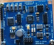
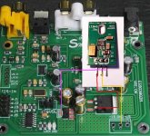
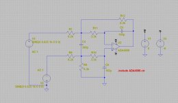
Have some pics showing the path of the I2C bus between AK4137 and MCU on the low cost AK4137 board. Since this board already has a slave output mode setting, the only remaining issue should be to change the output mode from PCM to DSD. Those particular settings are in the AK4137 internal I2C accessible registers.
Other pins that program it into slave mode are CM0 - CM3, which are set by the MCU writing bits to a 74HC595D chip on the pcb. If we wanted to control those bits too, we would need to get access to three signals that control the 'HC595. However, hopefully the MCU won't mind too much if we grab the I2C bus. So long as the MCU doesn't go bonkers and change the 'HC595 or something else to cause a problem, we might be able to test master mode DSD only getting control of he two I2C signals SDA, and SCL.
SCL in marked in yellow color in the pics, and SDA is marked in orange. Where the traces pass under the bottom side of the board, the paths are shown schematically on the top with yellow or orange lines with a black stripe down the middle.
The problem at this point will be to figure out how to cut the I2C connections and route them to a seizure relay so we can take control of the AK4137 at the right time to switch it to DSD mode.
Attachments
Here is a report on my progress with my V 1.07 ES9038Q2M board. Today I moved it into my main system to try out the I2S input from the Wave IO, and to compare it to a AK4490 dac from JLSounds. I was able to get to play DSD at 32 bit using Foobar with no problems. It sounded very nice and crisp, nice vocals, imaging, and sound stage, really great for a 40 dollar board. Piano tended to sound a little brittle compared to the AK4490 and it seemed to be a little more sibilant. The AK4490 sounded warmer, smoother, but not as crisp. All in all it compared very favorably with the AK. As for Opamps I settled on the LME49720 over the THS4032, I thought it sounded a little more open.
Now that I tested out the operability of the board I will try to do some modifications. The first thing I want to do it bypass the output capacitors. One member commented on what he did and stated to bypass R9 and R12 with 2K resistors to minimize DC offset when the output caps are bypassed. luckily I have some high tolerance 2K resistors in my parts bin, but I need some help in identifying R9 and R12. Can someone point me in the right direction ?
I also want to try out the regulator upgrade as shown in the attached pic, next.
Attachments
I need some help in identifying R9 and R12.
Not sure where you are getting the designators R9 and R12 from? Do you have a schematic you are referring to?
Regarding the regulator, maybe instead of replacing the existing regulator, you might keep it for powering the MCU and maybe DVCC. Getting the clock, VCCA, and AVCC onto a separate and higher quality regulator may be more helpful.
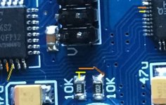
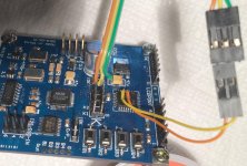
AK4137 modding is complete for now (pic below), at least enough to see if minimal modding can work for getting into DVD slave output mode. Will work on seizure relay and connection to Arduino next. Also, would like to capture some I2C bus activity for analysis during normal MCU control of AK4137, before proceeding to take control with Arduino.
Attachments
Not sure where you are getting the designators R9 and R12 from? Do you have a schematic you are referring to?
Regarding the regulator, maybe instead of replacing the existing regulator, you might keep it for powering the MCU and maybe DVCC. Getting the clock, VCCA, and AVCC onto a separate and higher quality regulator may be more helpful.
Hi Mark,
I had went through this thread and took screenshots of the comments on modifications that I thought that I could handle. Below are screenshots of the comments on R9 and R12 pertaining to removing the output caps. I don't have a schematic and I can see no designation of parts on my board. Unfortunately the screenshot doesn't show the comment number.
Paul
Attachments

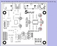
Schematic referred to is attached below. It's not exactly the same as the stock schematic of the dac board. Not sure if anyone ever posted the whole schematic of the stock output stage. Because the dac board is designed to work on +15v only, or + and - 15v, there is a bias network connected to the noninverting opamp inputs that makes them half way between V+ and V-, and V- is determined by either connecting a -15v supply, or by soldering J6 (?) to connect V- to ground.
Anyway, you could sketch out the output stage schematic easily enough if you want, and then see about modifying it to look like the attached schematic.
EDIT: Looks like that's the wrong schematic I found. I'll go looking again.
Anyway, you could sketch out the output stage schematic easily enough if you want, and then see about modifying it to look like the attached schematic.
EDIT: Looks like that's the wrong schematic I found. I'll go looking again.
Attachments
Last edited:
PJN,
Okay, I looked at how that attempt to get 0V offset at the output was intended to work. It is a not a great idea, IMHO. Looks like it was abandoned shortly after it was tried and the person went back to transformer output.
In any case, it is unlikely that sound quality would be significantly improved by such an approach. The problem with the stock output stage is not primarily in the output capacitors, they are the least of the problems, IMHO. If you want to redo the ouput stage somehow, may as well do something that is really going to help. Otherwise, I would suggest to leave the output caps they are. You could put some bigger caps in parallel if you want to play around, but again its not the problem, IMHO.
A fairly minimalistic approach was designed by a gentleman named Victor. However, it takes two opamps to make it work, one for each channel. He also made a minimal change to AVCC by soldering 3x 1800uf caps under the bottom side of the board to each of the existing AVCC filter caps. People say the extra AVCC caps helps some and its easy to do.
If you were interested in Victor's output stage, we could probably dig up the schematic, but why go to the trouble to improve it some using two opamps when you could improve it even more using three opamps (to get more filtering)?
Last edited:
Hi Mark,
Ok, I'll take your advice and abandon the output cap removal. Upon longer listening I think the 9038 seems to create a lot of high frequency emphasis that sounds expansive and exciting at first, but quickly gets fatiguing, probably do to the poor filtering in the output stage. The AK4490 sounds more realistic and much less fatiguing. It seems that the output stage should be addressed first.
I have a couple lme49710 opamps in the bin and I think that I remember taking a screenshot of Victors output stage. I'll study it and try my hand at putting it together on vero board. Since there is a socket for the opamp could it be as easy as removing the opamp and getting the correct inputs/output to/from the new output stage from the opamp socket ? If I run into trouble I'll give you a shout on this thread.
Paul
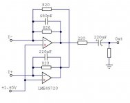
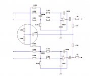
Victor's output stage would take four single opamps or two duals. A lot less trouble to implement with two LME49720. However, those and 49710 are sensitive to DECT cordless phone signals in the vicinity. OPA1612 don't have as much of an issue with that, also they are what I ended up with in the latest iteration of the modded dac. In addition, ESS uses them for 9038PRO evaluation boards. For this particular dac chip, I would use one of the two 49720 or 1612.
Victor's original output stage was as attached below. There is a later version that gets rid of the output caps. The 1.65Vref is one-half of AVCC for each channel. A voltage divider consisting of two 10k resistors and a 10uf filter cap on the output is needed for each channel.
EDIT: Found it. The 3.3v for each channel is from AVCC.
EDIT 2: The schematics don't show it, but proper opamp power bypassing with .1uf ceramic and 10uf tantalum for each power pin should be used. In addition, I keep finding that output stages sound better with a fair amount of stacked film caps on the 15v rails. They don't have to be super close to the opamps, but power wiring should be of pretty substantial gauge. I am currently using about 100uf of film caps per rail. Mouser carries Wima 33uf, 22uf, and 10uf, 63v leaded film caps that can be used to make up the filter. I find they help Katana dac a lot too when running its output stage from an external linear +-15v power supply.
Attachments
Last edited:
No problem, I'll pick up some of the 1612's. I'll study it and go through my parts bin to see what else I'll need to order
Please see EDIT 2, above. Recommend you add some film caps to the order if possible.
I think the 9038 seems to create a lot of high frequency emphasis that sounds expansive and exciting at first, but quickly gets fatiguing, probably do to the poor filtering in the output stage. T
Hi Paul,
Just to clarify what you might expect from an output stage, a proper I/V version with one or more real filter poles helps lot. Victor's design doesn't have any real poles, or enough poles at all for maximally clean and smooth sound quality. That is why I recommend adding one more dual opamp to make a total of three dual opamps for the output stage, as you can see from looking at the schematic for the output stage version I recommend.
However, with these dacs everything matters even the stuff the dac chip manufacturers say doesn't matter. It all matters. (paraphrasing pro audio designer Dave Hill.)
A low jitter clock helps. Upsampling helps to further reduce jitter. Conversion to DSD helps reduce certain PCM interpolation filter artifacts. Putting all dac chip power pins on appropriate separate voltage regulators helps. Master mode clocking or very low bandwidth DPLL settings help. Arduino tweaking of HD comp and DPLL registers helps, among other registers. Etc., etc.
You are right that a good output stage helps a lot, but not nearly so much without good AVCC supplies to go with it. (By the way, at perhaps some increase in cost, some labor can probably be saved by purchasing a TP AVCC voltage regulator board for ~$60 - $80. I haven't tried it, but it uses the same regulator chip parts Acko dac uses and is said to compare well with other high end options.)
It's all okay though, you will find out what changes and what you would still like to sound better as you work your way along, at least until you get tired of working or you decide it sounds good enough to satisfy you.
Last edited:
Hi Mark,
Right now it sounds good enough for my garage work shop, but I couldn't live with it in my main system. I'll try my luck with the various mods that you have outlined. Hopefully it will eventually better the other DACs I have in my nice sound systems, and if not I'll still have fun and hopefully learn something new along the way .
Paul
I had went through this thread and took screenshots of the comments on modifications that I thought that I could handle. Below are screenshots of the comments on R9 and R12 pertaining to removing the output caps. I don't have a schematic and I can see no designation of parts on my board. Unfortunately the screenshot doesn't show the comment number.
Paul
hi there,
to remove the output caps, here is the schematic and the components need to adjust.
there is only one set components for both opamps on the board, we neet 2 sets for the job.
cheers
Attachments
I wonder if you might be willing to say a little about how you arrived at your particular modding choices? Did you do much trial and error, or just come up with a plan and go for it, or maybe something quite different?
It is interesting to me that you decided to keep the one opamp output stage using voltage mode, even though we know distortion is quite a bit higher that way. Guess you must like it okay, otherwise you probably would have changed it. Wonder if you ever tried Victor's approach to an output stage?
hi, there,
my modding choices are just keep it simple, don't make things complicated unless it necessary. r-pi >>> i2s >>> 90x8 is the shortest path, putting anything in between them would incur additional fussy or adding distortions.
RPi and USB DAC's vs. I2S : DACs - Volumio
posts: 3934
it's understandable voltage mode opamp output stage is not perfect, but the improvement is subtle use other opamp schematic design. i'll try tango nn-600-50k or tango np126 line output transformers later.
merry christmas
Hi Mark,
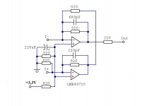
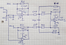
Is this the output stage that you recommend ? If I'm going to all of the trouble to build an output stage on vero board I might as well go all of the way to add a few more components. I haven't done this before so I want to make sure that I understand what's going on. Dac input is the + out from the dac channel and Dac B is the - out from the dac channel. The first two opamps are really the different halves of one double opamp like the lme 49720. The last opamp is a single opamp like a lme 49710. And the ground is the power ground. And I need to make one for each channel. So I'll need two double opamps and two singles (or another double to do both channels). Am I on the right track ?
Paul
Attachments
- Home
- Source & Line
- Digital Line Level
- ES9038Q2M Board