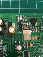
The 12,27 pins belongs to two VCCA pins of 9038Q2M
I have mentioned earlier, see post #1250.
thanks, any information if 12,27 pins connected internally?
Thank you eslei and janos_904 for reporting those modifications. Would anyone like to say how they think sound quality was affected, if at all, by non-AVCC power modifications? Reduced distortion, less noise, about the same, hard to say, etc.? Or, do we basically have reports that it was done but no other details are available?
thanks, any information if 12,27 pins connected internally?
I think they are connected internally. If you look at AVCC, there are actually two specific names, AVCC_L and AVCC_R. That suggests to me they are not connected internally. And, ESS says there should be separate regulators for left and right.
But VCCA is only one name, so those pins should all be the same thing and presumably are connected internally. That would be my understanding.
System 54, You could use a lower-than-100MHz ultra-low jitter, or ultra-low phase noise clock to help reduce jitter if you don't mind not being able to play higher sample rates. You would need to ask yourself some questions like these: What is the highest sample rate you would want to be able to play? Would you want to be able to use hardware upsampling at all? What about DSD capability, would you want that? If so, what speed DSD?
Once you determine what exact playback capabilities you would want, we could figure out the minimum clock speed you could use.
Once you determine what exact playback capabilities you would want, we could figure out the minimum clock speed you could use.
The schematic I used was identically the same as posted as by ESS document that Markw4 points out. The easy route is to use two dual op amps. Two LME49720s. Three would be for the IV stage and the fourth would be for the AVCC. The AVCC op amp stage is easy as pie and it works and a good AVCC is absolutely necessary.
This post shows when I was in the middle of laying it out on perf. I turn the perf upside down to make it easier to figure out what is going on. When I am soldering, it is obvious would be turned over.
ES9038Q2M Board If you will be using perf board similar to what is shown, get a pattern that has four or five connections perpendicular to the two perpendicular parallel rails. This will make the layout very simple and more compact. The parallel rails are used for the +/- 15V rails.
Had I not messed with the single op amp solution, my 9038q2m would possibly be close to Mark's. But now that proto board is idle. However, I still have most of the parts ready so it is possibly just another $40 or so to build another DAC. I'll wait and see what comes out of Katana. My HTPC video setup needs a good DAC not necessarily the best or close but a decent one. Once my 9028DAC started singing, my video setup started to be a real laggard. It's contagious. Be warned.
But again look at the circuit and it does not take a lot to make it. One afternoon and you're done. BUT when interconnecting between it and the board reread when I was connecting my hookup to the 9038q2m dac. Mark has a small error in one of his photos is identifying the DAC out lines. You will need to look at that closely and follow it. It would be good to see if someone else was able to pretty much replicate the results mark obtained.
Thank you Mikett. the picture were helpful. I understand it better than months ago
")
I think I will try to do the AVCC mod your way.
Looks like it is achievable with some little help.
I just received my new clock today.
As Mark told me it is bigger than the original one.
I will try to make some place for it without messing the board...
Attachments
@terry22, If you have not soldered SMD parts then I would suggest getting a practice kit such as one of these: smd practice solder kit | eBay
Then look for some SMD soldering instruction videos on youtube. There are some pro's out there that want to help you learn how.
As far as reading schematics that is only half the problem for construction from scratch. Layout is the other part that has to be figured out. Schematics show what connects to what, but not how the parts are physically arranged.
What I do is get a piece of graph paper and use each intersection of lines as representing a hole in my perf board, or a line may represent a solder trance on the SMD adapter board. I draw out how I will physically place parts in a way that makes sense. If using a foil ground plane, or strips of foil between IC sockets, something like that I allow for that too.
It is important to first think about how power wires and signal wires will be routed from stage to stage, from input to output. It is also important to keep opmap feedback components and power supply bypass caps as close to the IC leads as possible. So things come first in a prospective layout.
At the next level there is signal flow to think about. A signal comes into the circuit at some point often referred to as the input, gets processed by the circuitry, and exits out the output. Sometimes it is important were outputs are located, and sometime where inputs are located. For AVCC, I arranged the layout so the outputs where right next to the pins on the AVCC caps which were right next to the dac AVCC pins.
If you look at the pictures of my modded boards blown up all the way to full size you can see what my thinking was about how to address the concerns.
So, I usually do plan out layouts before I start soldering. I draw them up from schematics and then build them from the layout drawings. I find I get the best results that way.
Like anything else it get easier with a little practice and by looking at how other designers address the issues.
Thank you Mark for all the precious info.
I will order some practice kit.
Does some of you have a proper layout for Avcc to share?
What are the frequencies of the clocks you have? And do you have a data sheet for the SC cut clock? If so, what does it say for phase noise at 1Hz and 10Hz?
crystek cchd 575 22.5792 MHz and 24.576 MHz
phase noise of the driscoll sc clock is better than 120db/10hz
Without going to open any op-amp debate, I would like to ask if there is any chance of improvements if changing the su5 dac opamps, at RCA output, 1x op257 and 2x tl072 with the newer ADA4075-2. Analog devices states that this is the closest replacement for op275:
http://www.analog.com/media/en/news...letins-brochures/LPT-New-Product-Upgrades.pdf
http://www.analog.com/media/en/technical-documentation/data-sheets/ADA4075-2.pdf
there are also some reports that it can also replace the tl072 for what ever that means.
I do not have a clue if they can be direct replacements (probably not), but at least there might be a possibility of an alternative improvement, so that is why I note it here for research.
PS:Some notes on mobile low current devices: http://www.analog.com/media/en/technical-documentation/application-notes/AN-1429.pdf
Last edited:
Ok. Bad news this morning my board wasn't working anymore.
Blue leds were off.
After doing some measurement, it looks like the 7805 regulator is only sending about 1V and not 5V anymore.
the Vin is still 15V.
Do you think I just need to replace it, or it may have another cause?
Blue leds were off.
After doing some measurement, it looks like the 7805 regulator is only sending about 1V and not 5V anymore.
the Vin is still 15V.
Do you think I just need to replace it, or it may have another cause?
I just received my new clock today.
As Mark told me it is bigger than the original one.
I will try to make some place for it without messing the board...
The new clock will have to go where the old clock is. That means the old clock will have to come out. No hurry on that. Best to get some practice on easier things first.
After doing some measurement, it looks like the 7805 regulator is only sending about 1V and not 5V anymore.
the Vin is still 15V.
Either something is drawing a lot of current or the regulator is bad, it sound like.
Does anything on the board feel warm to the touch? Sometimes filter caps can short. About the only thing that loads the 5v supply is the 3.3 volt regulator.
The difficulty with troubleshooting what might be a bad regulator or what might be a short somewhere is that you typically need to cut traces or remove components to figure out the problem.
You could also try turning off the power a measuring for a short to ground at the output of the 5v regulator. If you do find a low resistance to ground you could start by lifting the output pin of the regulator or cutting it and seeing if that changes anything. The short could be inside the regulator or outside of it.
If you don't find any low resistance to ground at the output of the 5v regulator that could mean the regulator is bad, or that it takes more voltage that a multimeter puts out to cause high current draw.
if you have another 5v power supply you could lift the output pin of the regulator and use another 5v power supply to power up the 5v bus and see if it comes back to life.
Also, maybe good to know that the 5v regulator only feeds the 3.3v regulator and the 5v power hole/pin at the I2C terminals.
Probably the preferred approach would be to try measuring for low resistance loading first and if nothing found then substitute another 5v supply. If you have a higher current 5v supply that might heat up anything causing a short or heavy load on the 5v but, or it might cause something to open like of fuse. If you proceed carefully chances are good you can fix it okay.
Just remember if you lift the 5v regulator output and apply +15 power to the board then the regulator might oscillate without an output capacitor hooked up to it. For that reason cutting a trace after the output capacitor might be a better place to interrupt the circuit.
Also, it should be possible to hook up another 5v supply without turning on the +15v power. In that case the +-15v would only be needed by the opamp which won't be hurt if the 5v is on. Or you could pull it from the socket.
EDIT: it could be andora76 suggestion is good too, although sometimes you can see a regulator that fails only with more loading than 10k. So, you might have to come back and look at that again if you don't find anything else. There is more than one way to start troubleshooting something like this.
Last edited:
@pentajazz, There are more problems with that part of the circuitry than opamp swaps can fix. It needs higher current, higher speed opamps to work properly, IMHO. But that means it would need better ground plane and power decoupling to prevent instability. Also, the ground return the DAC chip is just insanely bad. You might be able to cut the grounding somewhere and add copper foil to make a ground plane back to the DAC chip directly from the output stage. Also use copper foil to make ground plane under the board where the output opamps are. Put mylar tape over the existing traces so they don't get shorted by the copper foil. Leave holes in the mylar tape and copper foil where there are through-hole component vias. That way you can still remove and replace parts. With faster opamps the film decoupling caps will probably need to be replaced with tantalums in parallel with ceramics. You might need to get the ceramics closer to the opamp power pins. Good opamps to use are LME497xx singles or duals as needed to replace what is in there. To get the old opamps out and the new ones in you will probably have to remove most of the film caps anyway in order to get access to solder.
After finishing the above you might want to fix the +-15 power quality and AVCC supply. Then you should start hearing quite a bit of improvement.
After finishing the above you might want to fix the +-15 power quality and AVCC supply. Then you should start hearing quite a bit of improvement.
Last edited:
@MrSlim, I am trying to decide whether to disassemble my test setup to put the new SRC in there or wait to do the new firmware Allo Katana comparisons first. Reviewer Katanas are expected to be along later this week. Most likely one way or another I should be able to get the new SRC in there by early next week.
- Home
- Source & Line
- Digital Line Level
- ES9038Q2M Board