Hi Mark
thanks for all the info , could you give the link for the board above by any chance?
Please note there are three different versions. I have the 'standard' one. AK4137 I2S/DSD Sample Rate Conversion Board Supports PCM/DSD Interconversion DOP | eBay
@terry22, If you have not soldered SMD parts then I would suggest getting a practice kit such as one of these: smd practice solder kit | eBay
Then look for some SMD soldering instruction videos on youtube. There are some pro's out there that want to help you learn how.
As far as reading schematics that is only half the problem for construction from scratch. Layout is the other part that has to be figured out. Schematics show what connects to what, but not how the parts are physically arranged.
What I do is get a piece of graph paper and use each intersection of lines as representing a hole in my perf board, or a line may represent a solder trance on the SMD adapter board. I draw out how I will physically place parts in a way that makes sense. If using a foil ground plane, or strips of foil between IC sockets, something like that I allow for that too.
It is important to first think about how power wires and signal wires will be routed from stage to stage, from input to output. It is also important to keep opmap feedback components and power supply bypass caps as close to the IC leads as possible. So things come first in a prospective layout.
At the next level there is signal flow to think about. A signal comes into the circuit at some point often referred to as the input, gets processed by the circuitry, and exits out the output. Sometimes it is important were outputs are located, and sometime where inputs are located. For AVCC, I arranged the layout so the outputs where right next to the pins on the AVCC caps which were right next to the dac AVCC pins.
If you look at the pictures of my modded boards blown up all the way to full size you can see what my thinking was about how to address the concerns.
So, I usually do plan out layouts before I start soldering. I draw them up from schematics and then build them from the layout drawings. I find I get the best results that way.
Like anything else it get easier with a little practice and by looking at how other designers address the issues.
Mark has a small error in one of his photos is identifying the DAC out lines.
To clarify what Mike is referring to, at the time I first marked up a picture of the DAC circuit board showing where the DAC outputs go, it was before we had access to the the ES9038Q2M data sheet or a pinout diagram, so I got the phases reversed. That is what is sometimes called DAC or DACA is really DACB, and what is labeled DACB is really DAC or DACA.
Does it matter? It shouldn't, I don't think. It is a phasing thing. On is the inverting dac output and the other is non-inverting. Both should go through I/V stages for best results then summed using a differential amplifier circuit to cancel out common mode offsets and distortion. That way the output of the differential stage should be quiescently at ground, which means you can get by without output coupling caps if you want. It's not quite as good as servoing the output to ground, but I do not find any problems with DC offsets with my DAC. However, it is important to use tight tolerance SMD thin film resistors. That's why I recommend learning how to solder them and work with them before using good parts on a board you will be using for a long time (hopefully).
Also, as it turns out larger size SMD parts can be soldered to the pads on standard perf board. I don't use the type of perf board with strips of copper on it, only the kind with solder pads on both sides and plated through holes. The solder pads can be used to solder down ground plane after sockets are installed and through hole parts are in place. After through hole parts and ground plane is done, then signal power power wires can be run on the top or the bottom of the board. I might run power on the top and leave some holes in the ground plane to bring down near socket pins where it will be needed. That leaves lot of room on the bottom of the board to run signal wires. The ground plane can be on the top of the board or the bottom, but plan how you will solder leads from decoupling caps to it while keeping the leads as short as possible. If you want I would probably take some picture of a notch filter I constructed that way. It isn't so tiny as what I did for the modded DAC boards.
Thought I might share a few evolving thoughts on jitter and upsampling. First, there is an ESS paper describing some technical aspects of Sabre dacs here: http://www.esstech.com/files/4314/4095/4318/sabrewp.pdf As can be seen, among other things they describe some different types of jitter as well as some some ways jitter can affect sound quality. The takeaway would seem to be that jitter can be a very non-stationary type of non-linear distortion. For example, it can add noise that results in distortion perhaps only during brief moments when there are big changes in music dynamics, say, from soft to loud, possibly as occurs in the presence of uncompressed percussion instrument sounds. So, its effects can be hard to characterize using techniques that work well for more stationary types of harmonic distortion. In addition, the effects of jitter can definitely be audible, but to what extent may depend in part on listener sensitivity.
Regarding upsampling, it seems to benefit sound quality in practical effect by reducing jitter, but that leaves a question as to why hardware upsampling seems to work better than software upsampling. My suspicion would be that software upsampling might reduce jitter in the same way hardware upsampling does, but the problem would then be that jitter could then be reintroduced as it makes its way by various means to the dac hardware inputs. The benefit of hardware upsampling would presumably be that it can be the last thing that happens immediately before the signal arrives at the dac inputs. Of course, it could still be possible for some jitter to be reintroduced as signals make their way from upsampler hardware to dac inputs. Also, there may be some limitations as to how much jitter attenuation a hardware upsampler can provide, and how much of its own jitter might be imparted on a signal.
As a practical matter, we can use good practices to transport uspampler output signals to dac inputs. In addition we can try to minimize upsampler jitter by use of high quality power and decoupling practices, as well as use low jitter clocks for upsamplers.
Assuming we are able to present a very low jitter input signal to the dac, the next question might be what happens inside the dac with any remaining jitter. Sabre dacs attempt to remove any remaining jitter but the resulting quality of that effort is affected by DPLL loop bandwidth. To achieve the best possible audible benefits from low jitter Sabre dac input signals DPLL bandwidth must be set the lowest stable setting.
Beyond the foregoing, there seems to be at least one additional factor operating in hardware upsampler and dac interaction. With Sabre dacs it appears that upsampling to DSD rather than PCM may result in better sound quality. In that regard, there are a couple of factors within Sabre dacs of possible note. DSD DPLL bandwidth by default has a larger range of possible reduction settings as compared to PCM/I2S settings. Another factor in Saber dacs is that PCM/I2S passes through a first stage of FIR upsampling reconstruction/interpolation filtering before passing through 2nd stage IIR filtering. DSD on the other hand only passes through IIR filtering. Bottom line, for whatever less than fully understood reasons hardware upsampling to DSD format seems to allow for better sound quality than if using PCM/I2S format.
Of course, hardware upsampling architecture with Sabre dacs as described in this thread is only one possible dac system architecture. The approaches taken by Benchmark DAC-3 and Allo Katana are architecturally different from what is described in the this thread and also different from each other. There is more than one way to skin at cat, as it were, but whatever approach is used there are probably many more wrong ways to do it than right ways. Great care and attention to implementation details is necessary no matter which approach is used in order to obtain best sound quality results.
Last edited:
More high value snippets of information regarding output stage implementation from John Siau here :
Review and Measurements of Benchmark DAC3 | Page 16 | Audio Science Review (ASR) Forum
Review and Measurements of Benchmark DAC3 | Page 16 | Audio Science Review (ASR) Forum
Hi abraxalito, Thank you for that link.
To follow up a bit on something we discussed previously, I now have the ES9038PRO data sheet, and the ES9038PRO evaluation board schematic. They are still using opamps for IV output stages as it turns out, but this time OPA1611. They are also still showing the IV opamps loaded with less than 600 ohms. I continue to assume that must be possible due to current draw being limited by actual operating output swings.
They do say somewhere in something I read that there are limits to how low one can go with resistor values without adversely affecting opamp distortion performance so I assume they are not being super stupid and are actually measuring and listening to what they design. That being said I am not equipped to independently verify how well it works.
So, I am still kind of guessing that data sheet graphs or tables of distortion as a function of output load resistance must be taken at some standard voltage swing or maybe some standard percentage of Vcc, something like that. Otherwise, I don't see how to make much sense out of the information available.
Last edited:
It should have one AVCC regulator for AVCC_L and one regulator for AVCC_R. I used one LME49720 dual opamp for that. If you wanted to try that opamp, you might download the data sheet and and look at the pinout. Also, if you look at the picture of the bottom of my modded DAC board, you can see how I laid out the opamp, power bypass caps, and dedicated 3.3v voltage reference shared by both AVCC supplies. In addition, the picture shows where the two sets of voltage dividers and filter caps to produce the output stage reference voltages is located right next to the AVCC opamp.
The picture of the AVCC regulator I made is here: http://www.diyaudio.com/forums/digital-line-level/314935-es9038q2m-board-38.html#post5377834
If you have any questions about what any of the components in the picture are for please ask.
EDIT: Also, the 3.3v regulator I used as an AVCC reference (and also used one as a voltage regulator for the clock oscillator) is an LT1763CS8-3.3PBF. Think I may have also used one of those to power the microcontroller (just to put it on a separate regulator as per ESS suggestion). Connected it up according to the data sheet for lowest output noise. That requires one extra C0G cap besides the usual X7R input and output caps.
The little wire shown in the picture going over to the 1.2v regulator on the top of board is no longer there. At the time I modded that part of the circuit I didn't have the data sheet for the dac chip, so I didn't know for certain what was or wasn't needed there. In other words, it was a guess.")
The picture of the AVCC regulator I made is here: http://www.diyaudio.com/forums/digital-line-level/314935-es9038q2m-board-38.html#post5377834
If you have any questions about what any of the components in the picture are for please ask.
EDIT: Also, the 3.3v regulator I used as an AVCC reference (and also used one as a voltage regulator for the clock oscillator) is an LT1763CS8-3.3PBF. Think I may have also used one of those to power the microcontroller (just to put it on a separate regulator as per ESS suggestion). Connected it up according to the data sheet for lowest output noise. That requires one extra C0G cap besides the usual X7R input and output caps.
The little wire shown in the picture going over to the 1.2v regulator on the top of board is no longer there. At the time I modded that part of the circuit I didn't have the data sheet for the dac chip, so I didn't know for certain what was or wasn't needed there. In other words, it was a guess.
Last edited:
...make sence to implement the avcc circuit also for the vcca?
No, not necessary for VCCA. Although, you could put both of the VCCA pins on one additional LT1763CS8-3.3PBF 3.3v regulator if you want. Something like that. It could help to isolate them from digital noise on the board's built-in 3.3v supply.
Last edited:
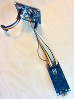
Spent most of the morning making up cables to try out the new, low-cost AK4137 upsampler. This one, as some may recall, only has I2S/PCM/DSD inputs. No SPDIF, TOSLINK, or AES.
Another thing about this board is they didn't lay out the connectors very sensibly for what it is supposed to interconnect with. The other, more expensive AK4137 is much better in that respect. Pics below (display not shown).
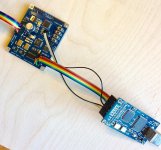
EDIT: Added pic showing extra ground pins I added for I2C/PCM/DSD interconnects. The added ground pins are yellow color.
Another thing about this board is they didn't lay out the connectors very sensibly for what it is supposed to interconnect with. The other, more expensive AK4137 is much better in that respect. Pics below (display not shown).
EDIT: Added pic showing extra ground pins I added for I2C/PCM/DSD interconnects. The added ground pins are yellow color.
Attachments
Last edited:
@eslei, we definitely do use separate regulators for AVCC_L and AVCC_R, as ESS strongly recommends.
However, those two regulators (made from a dual opamp on my own board) may use a shared voltage reference source, which is fine. It does not cause cross-talk between the channels.
As you seem to know, what should be avoided if possible is using one AVCC regulator for both right and left channels. Unfortunately, some ES9028PRO boards are wired to work with only one AVCC regulator and the traces are buried inside a multi-layer PCB making it very hard to fix.
Also, you are very welcome for the information I post here. I want to help people be able to have better dacs if possible. Unfortunately, it can be a lot of work to mod one fully, but they can sound incredibly good when finished. I think it is probably worth the effort to do it once at least.
Last edited:
Hi Mark.... any comments on improvements I could attempt on this board ??
Es9028Q2m with I/V and lpf implemented as stock.
ES9028Q2M ES9028 I2S input decoder board mill board DAC balanced output | eBay
Thanks,
bob.
Es9028Q2m with I/V and lpf implemented as stock.
ES9028Q2M ES9028 I2S input decoder board mill board DAC balanced output | eBay
Thanks,
bob.
@bob, Don't know about that board. Don't have a data sheet for ES9028Q2M either. If you had a schematic and some in-focus close-up pictures of the component side and the solder side we would know a lot more. Right now I can't even see a clock in the pictures. There might not be any ground plane on the bottom either, who knows. A very rough guess would be with about $200 in parts and a month's work you maybe could end up with something pretty decent. But, you would be likely more or less starting from scratch. At least we already know a lot about how to mod the ES9038Q2M board in this thread. But, if somebody wants to get one of those ES9028Q2M boards, it would be nice if they would post good pictures here and then we could say more about it.
Last edited:
@ markw4 i am talking about vcca, on 9038q2m pin 12 and pin 27, according to 9038q2m datasheet they are analog core ps inputs. i don't have es9028q2m datasheet, but still can identify them from pcb. i got only two ohms between two pints, they may connected internally. the datasheet didn't mention this, i make each a separate regulator anyway.
@eslei, Oh, I'm sorry! I know what you mean now. I could see putting both VCCA pins together on one separate regulator to get them more isolated from digital noise on the other 3.3v lines, but ESS doesn't say anything about it that comes to mind at the moment.
So, you put each VCCA pin on it's own regulator? If so, why? And, in what way did it sound different after that?
Actually, the more I think about it I'm not sure it would be a good idea to use two regulators for that. If there is a low resistance between the two pins and the regulators are at slightly different voltages then there would be some current flowing out of one regulator, through the dac chip, and back out to the other regulator. See what I mean?
Last edited:
The 12,27 pins belongs to two VCCA pins of 9038Q2M@ markw4 i am talking about vcca, on 9038q2m pin 12 and pin 27, according to 9038q2m datasheet they are analog core ps inputs. i don't have es9028q2m datasheet, but still can identify them from pcb. i got only two ohms between two pints, they may connected internally. the datasheet didn't mention this, i make each a separate regulator anyway.
I have mentioned earlier, see post #1250.
I have posted later #1584, the DVDD of 9038Q2M chip is supplied internally from DVCC. What all you need just a 4.7 uF X7R decoupling capacitor at the DVDD pin.i have ver 1.04 with ldo, but no change after pinoff the ldo.
dvdd still has 1.27v
Last edited:
- Home
- Source & Line
- Digital Line Level
- ES9038Q2M Board