Did you have to use a ground loop breaker or something to prevent hum?
I tried to make everything double insulated, so I didn't have to connect the enclosure to protective earth (which would have been difficult anyway as the enclosure is made of wood). I live in an old Dutch house where most outlets have no protective earth.
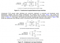
As the circuit is balanced and transformer coupled, I think it should be possible to get rid of ground loops even if it were built into a metal enclosure connected to protective earth and it were driving an unbalanced input of an earthed amplifier. In accordance with AES48, the enclosure could be connected to the internal circuitry at only one place and pins 1 of the XLR connectors could be connected straight to the chassis. When you then connect pins 2 and 3 to the amplifier, there is no ground loop.
I used transformer coupling for the S/PDIF inputs. No idea if it was really needed.
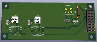
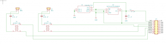
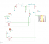
I'm trying to come up with a little PCB for the three non-USB inputs I want. My plan is to do BNC, AES, and optical. The BNC and AES ports will plug into J1 and J2.
C1 and C2 are 0.01uF capacitors, T1 and T2 are Scientific Conversion SC947-02, U1 is a SN74LVC1G125DBV buffer/line driver, L1 is a 47 uH inductor, C3 is a 0.1 uF capacitor, and the optical port is an Everlight PLR135/T10. This would mean that on the Valve DAC PCB, R30 and R31 are going to be 75 and 110 ohm, respectively. the P7 on this board corresponds to P7 on the Valve DAC, so I was hoping to get the 3.3 V for the optical receiver from pin 1. Does this look alright? I also think that for the BNC input, that I connect the RX minus to ground? But not for the AES?
C1 and C2 are 0.01uF capacitors, T1 and T2 are Scientific Conversion SC947-02, U1 is a SN74LVC1G125DBV buffer/line driver, L1 is a 47 uH inductor, C3 is a 0.1 uF capacitor, and the optical port is an Everlight PLR135/T10. This would mean that on the Valve DAC PCB, R30 and R31 are going to be 75 and 110 ohm, respectively. the P7 on this board corresponds to P7 on the Valve DAC, so I was hoping to get the 3.3 V for the optical receiver from pin 1. Does this look alright? I also think that for the BNC input, that I connect the RX minus to ground? But not for the AES?
Attachments
Last edited:
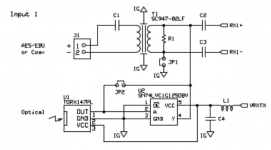
The recommended application circuits from TI for the DIX4192 AES3 and S/PDIF inputs are as shown in the attachment. Note that the pins of the XLR connector are drawn in the wrong order, pin 1 is never in the middle. TI recommends 0.1 uF for C1 and C2.
I think the secondary of the AES3 transformer can not be grounded on one side because that would make the level on the other side too high to handle for the DIX4192. An AES3 level can be as high as 3.5 V peak differential into 110 ohm, while the DIX4192's I/O supply is 3.3 V nominal. It probably just fits when the positive and negative signal swings are equal but opposite.
There is no such issue for S/PDIF, but I have no idea what advantage grounding one side has over not doing so. Apparently TI has the experience that there is some advantage or other.
The application circuit also shows one side of the S/PDIF transformer's primary grounded, but that makes no sense when you want to prevent ground loops. In my build, I mounted the transformers very close to the input connectors and didn't ground either side of the primary.
The buffer behind the optical receiver may be a very good idea, as the receiver datasheet isn't very clear about what loads it can drive. I have no such buffer, but the one time I wanted to use the optical input, it actually didn't work (could also be due to the source driving the optical cable, I don't know). You can tap off the 3.3 V from the valve DAC. I would recommend reserving space for a resistor between the buffer's output and the cable to the main PCB, so you can terminate the cable more or less characteristically at the driving side.
Attachments
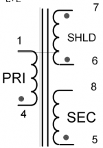
I will take a look at the DIX4192IPFB datasheet and edit my schematic. I was copying the inputs from the Gamma 3 DAC that I have because I don't have any actual EE knowledge lol. All of the part values are from that part list. On that DAC, I think the transformer is grounded, and it's labeled "shield" on the data sheet. I left pins 2 and 3 floating.
Attachments
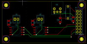
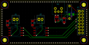
After looking at the DIX4192 datasheet, I realized that my configuration was for a 5 V optical receiver, but my selected part is a 3.3 V, so the buffer is not needed. I fixed the schematic to follow Figure 74 from the datasheet. I am also no longer using RX4P, since U6 seems to also be suited for 5 V inputs. The PCB has dual ground planes now as well.
Attachments
The 74LVC1G34 (U6) between pin 3 of connector P7 and pin 7 of the DIX4192 on the original valve DAC main board is meant as a level shifter, to make it compatible with both 3.3 V and 5 V optical receivers. I don't know how long a cable the optical receivers can drive, though. A buffer right next to the receiver may or may not be useful when the connection between the receiver and the main board is long.
The datasheet says the receiver can drive a max of 5m, and I plan on making the connecting cable as short as possible. I guess adding the buffer back in isn't much effort. As far as the ground, I should only connect one of the ground pins back to the Valve DAC, correct?
There is a transmission distance d = 0.2 m to 5 m specified in the optical receiver datasheet, but I assume that relates to the length of the optical cable rather than the electrical cable. The specifications at 3 V are with a 5 pF load, which means just a few centimetres. All in all, I think the buffer and output termination resistor are required, or at least they won't harm.
I also may have to retrofit a buffer in my own valve DAC. My optical receiver (Cliff FC684208R) is specified for 10 pF load and I'm pretty sure the cable it drives has much more capacitance than that.
Regarding the ground pins, I would connect all of them to have a reasonable RF ground connection and some shielding between the signal lines. That creates ground loops, of course, but assuming you use a flatcable, they will have very small loop areas and any hum currents they pick up will not flow anywhere near the analogue audio parts.
Last edited:
The one I wrote about in post #1383. I think it's a good idea to put a resistor between the buffer and the cable to the main board, probably of the order of 82 ohm, to prevent cable resonances. Neither the buffer nor the resistor is needed when the optical receiver is just a few centimetres from the DIX4192, as is probably assumed in the DIX4192 datasheet.
Last edited:
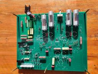
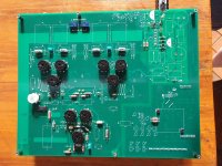
Two days of soldering and everything is populated apart from a handful of power supply caps that are yet to arrive. Went a bit stupid ordering resistors but in the pre and power amps I've built any resistor or capacitor on the grid/anode/cathode of the valve makes a difference to the sound and I have no reason to believe it would be any different in the ValveDAC.
Have put any of the taller through-hole components underneath the pcb so I can maximise the height of the valves protruding from the top of the case. Basically started with the necessary parts such as the trimpots and anything taller had to go down below.
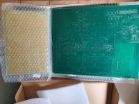
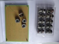
Even managed to wind 24 inductors for two filter boards for 6th order "0.05deg Linear Phase" and "Gaussian to 6dB"...except I dropped one and shattered a ferrite core half so will have to reorder that part. Was going to solder everything to the filter pcb's but was struck by how little metal there is around the holes. Is this normal? Can someone with leadbelly pcb's please have a look and let me know, that would be great. Might have to give the fab house a phonecall to get them re-done if necessary. No issues at all with the pcb for the dac.
Have put any of the taller through-hole components underneath the pcb so I can maximise the height of the valves protruding from the top of the case. Basically started with the necessary parts such as the trimpots and anything taller had to go down below.
Even managed to wind 24 inductors for two filter boards for 6th order "0.05deg Linear Phase" and "Gaussian to 6dB"...except I dropped one and shattered a ferrite core half so will have to reorder that part. Was going to solder everything to the filter pcb's but was struck by how little metal there is around the holes. Is this normal? Can someone with leadbelly pcb's please have a look and let me know, that would be great. Might have to give the fab house a phonecall to get them re-done if necessary. No issues at all with the pcb for the dac.
Attachments
Last edited:
- Home
- Source & Line
- Digital Line Level
- Valve DAC from Linear Audio volume 13