So long as there isn't a Guardian DAC.
Are you afraid they might team up and take control of all the audio equipment in the world?
Yes, I was being rather tongue in cheek Marcel. Anyway, my listening room wouldn't be big enough...
I know you were kidding, but still I wanted to explain why I thought of making a softcore Pilot ACE emulator rather than a Colossus emulator. The Pilot ACE is Turing-complete and based on Turing's design.
As far as I remember, the real Pilot ACE is not nearly as big as Colossus, by the way. I saw the rebuilt Colossus in The National Museum of Computing on Thursday 11 June 2015 and the Pilot ACE in the Science Museum in London one day earlier (or later, but I think earlier).
All the bits for my build are either here or ordered, apart from a case, which I will build from scratch once I get an idea of exactly what needs to fit within. Transformers seem like they will be the hold-up, both power and output. Freight comes in as a large part of the overall cost when you live on the opposite side of the world to where the bits need to come from in dribs and drabs.
Am looking forward to the build.
Am looking forward to the build.
A visit to Bletchley is still on my 'bucket list' - it should have been last summer but...
Such a shame that so much of the original Bletchley kit was apparently destroyed in 1945/46 - imagine thinking that you could put the genie back in the bottle.
Anyway, if things improve maybe this summer, coupled to a visit to the Shuttleworth Collection (pretty sure I mentioned that to you before);
Shuttleworth Collection | Shuttleworth
Are you afraid they might team up and take control of all the audio equipment in the world?
We should be so lucky that they would stop there.
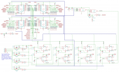
This is my proposal for a 4:1 I2S multiplexer, version with only 3.3 V CMOS inputs. It can be changed into LVDS for BCK, LRCK and data (SD) by replacing the A sections of the 74LVC244As with a quadruple LVDS receiver with three-state CMOS outputs, such as the SN65LVDT390ADBT. The 74LVC74A's are meant to ensure safe clock switching for the bit clock. The 74HC14 debounces the signals from the switch. C8 and C9 are meant to prevent hold time issues. Use at your own risk, as the circuit has not been tried, tested or simulated.
Attachments
Last edited:
I forgot to mention explicitly that the circuit of post #1347 is meant for the original valve DAC, where the signal first goes into an FPGA module, then into an asynchronous sample rate converter, then back into the FPGA module, then gets reclocked twice by flip-flops and then gets retimed by a current-steering valve logic gate.
For the raw DSD valve DAC, I would recommend a clearer separation between the data handling and the clock handling part. Unfortunately that would probably lead to a larger skew, as the data and bit clock or master clock can't be buffered by the same ICs when you want to keep them well-separated. It may then be necessary to add extra delay circuits and/or reclocking flip-flops to solve hold time issues.
For the raw DSD valve DAC, I would recommend a clearer separation between the data handling and the clock handling part. Unfortunately that would probably lead to a larger skew, as the data and bit clock or master clock can't be buffered by the same ICs when you want to keep them well-separated. It may then be necessary to add extra delay circuits and/or reclocking flip-flops to solve hold time issues.
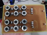
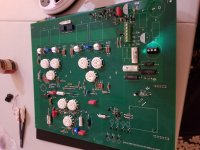
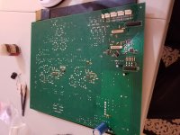
Making some progress! Everything installed other than output caps, the voltage regulators, and the lights (since I need to decide how to do those).
I've got a Maida PSU and a Pete Millett supply for the 6.3V. Just need to get the transformers, cases, and FPGA.
Might have wasted money on a voltage regulator, because I forgot that the FPGA will increase the power draw on the 5V rail. Went with this regulator, but it's max current is only 500mA. Will probably just go with the L4940V5 and save the fancy once for something else.
Attachments
Sonny, regarding the voltage regulator current rating, that vendor (there will be others I'm sure) has LT3045 regulators that uses them paralleled for higher current;
LT3045
This vendor is the source of the regulator I use in my DSD version build, albeit the 500mA version, and I have used his regulators in other projects - they're good.
LT3045
This vendor is the source of the regulator I use in my DSD version build, albeit the 500mA version, and I have used his regulators in other projects - they're good.
Looks great! How did you do the fine-pitched SMD soldering?
I oversized the 5 V supply a bit, because I didn't know what would happen when I changed the configuration file or how much sample-to-sample spread there would be. The last time I measured it, the current drawn from the 5 V supply was three hundred something milliamps if I remember well, but that was several configuration file updates ago. So your LT3045's current handling may or may not be sufficient.
I oversized the 5 V supply a bit, because I didn't know what would happen when I changed the configuration file or how much sample-to-sample spread there would be. The last time I measured it, the current drawn from the 5 V supply was three hundred something milliamps if I remember well, but that was several configuration file updates ago. So your LT3045's current handling may or may not be sufficient.
Looking good Sonny! This is the first I've seen the pcb up close with some bits on it. Interesting to see just where the vertical resistors and some of the other taller components are located on the board.
You've not soldered on the 7 pin valve socket yet...perhaps you purchased a rubbish one like me where the pin sockets are too tight to push in the valve pins.
Marcel, is there likely to be a performance improvement with use of these ultra-low noise 5V regulators considering their output ends up in places like the clock and the flip-flops in the dac cores? I've not made my mind up how to proceed to be honest and have a number of options available but it looks like a "definitely maybe" to me.
I don't think so. I'd expect the noise of the regulator to be negligible compared to the switching spikes of the FPGA anyway, despite the frequency planning: as much as possible of the FPGA runs on clock frequencies that cause no interference when they should end up on the DAC reference or clock, but even then there are data-related sidebands. The flip-flops that drive the upper E88CC's run on -132 V and -137 V, so not on the 5 V supply.
Sonny, regarding the voltage regulator current rating, that vendor (there will be others I'm sure) has LT3045 regulators that uses them paralleled for higher current.
I already ordered the 500mA one a few weeks ago, I think I'll just go with the recommended part since it's only $1 and won't negatively impact performance.
You've not soldered on the 7 pin valve socket yet...perhaps you purchased a rubbish one like me where the pin sockets are too tight to push in the valve pins.
That was not by choice lol, I ordered it with the others and the seller must have forgotten it. I'll order one when I get my tubes. Four resistors are also missing because I messed up when ordering. I also did not install the 75 or 110 ohm resistors yet, because I'm not sure what my input configuration will be.
Looks great! How did you do the fine-pitched SMD soldering?
I used a magnifying glass and a conical tip on my iron. Put some flux down, then put a tiny bit of solder as close to the tip as I can, and barely touch the pads one at a time. They are so small, they heat up quickly, and the solder fills up the pad easily. Just had to watch for bridging, which I did have one but resolved it.
I don't think so. I'd expect the noise of the regulator to be negligible compared to the switching spikes of the FPGA anyway, despite the frequency planning: as much as possible of the FPGA runs on clock frequencies that cause no interference when they should end up on the DAC reference or clock, but even then there are data-related sidebands. The flip-flops that drive the upper E88CC's run on -132 V and -137 V, so not on the 5 V supply.
The benefits of your well planned design. It looks like the clock 5V could be completely separated from the remaining 5V with omission of the L6 inductor and I assume that inductor is there to hunt a little noise from getting through to the clock.
I remember reading about the PSAudio Directstream Dac years ago and that the FPGA was considered a major source of noise within the unit, a significant contributor to its relatively pedestrian noise measurements. I may be wrong, or mis-remembering, but perhaps some of that FPGA noise in the ValveDac could be pacified with a power supply capable of reacting well to rapid current fluctuations...something with a large ultracapacitor at output. I remember seeing a scope reading showing the effect of an ultracapacitor filter at the output of a LDO that was subjected to rapid current pulsing...it looked to have made a significant improvement.
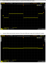
You could indeed remove L6 and use a separate 5 V supply for U17. Any jitter caused by ripple on the 5 V for U17 is supposed to be suppressed by the current steering gate made of E88CCs, but that suppression is imperfect, so maybe a separate supply or separate regulator could improve performance to some extent. I don't know, as I haven't tried it, but it certainly makes more sense than using an ultra low noise regulator for supplying an FPGA board.
For suppressing really rapid current variations, physically small capacitors work best. Hence the use of 10 uF X5R SMD capacitors at various places.
Regarding noise, as reported in the Linear Audio article, I measured noise floors of -85.76 dB(A) left and -91.29 dB(A) right with respect to a full-scale sine wave in the PWM8 mode. That's low enough not to bother me at all, but not nearly as low as some solid-state DACs.
- Home
- Source & Line
- Digital Line Level
- Valve DAC from Linear Audio volume 13